SK Hynix HBM4 Mass Production Begins — Samsung Showcases Competing HBM4 at GTC 2026
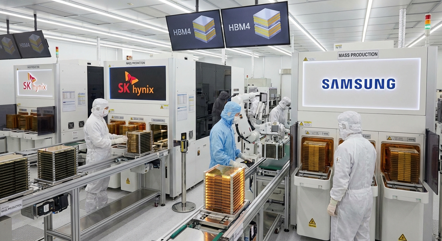
The race for next-generation high-bandwidth memory has entered production. SK Hynix has commenced mass production of HBM4, the fourth generation of its high-bandwidth memory technology, which offers substantially higher data transfer speeds and capacity per stack compared to HBM3E. The HBM4 specification supports up to 2 TB/s of bandwidth per stack with a 2048-bit wide interface, roughly double the bandwidth of HBM3E, while simultaneously improving power efficiency by 30% through lower operating voltages and advanced power management circuits. SK Hynix's initial HBM4 products feature 12-high stacks delivering 36 GB per module, with 16-high 48 GB variants expected by Q4 2026.
Samsung, not to be outdone, showcased its own HBM4 technology at NVIDIA's GTC 2026 conference, demonstrating working samples and announcing partnerships with multiple chip manufacturers. Samsung's approach differentiates itself through a hybrid bonding interconnect that eliminates traditional micro-bumps between memory layers, enabling tighter stacking pitches and theoretically higher bandwidth density. However, industry sources indicate Samsung's HBM4 yields are currently 15-20 percentage points below SK Hynix's, and full NVIDIA qualification is not expected until Q3 2026 at the earliest. The qualification gap has allowed SK Hynix to maintain its dominant 50%+ share of the HBM market, with Micron holding approximately 30% and Samsung trailing at 20%.
The HBM4 generation is critical for enabling the next wave of large language model training, where memory bandwidth has become as important as raw compute performance. Models with over 2 trillion parameters require massive memory capacity and bandwidth to efficiently distribute training data across GPU clusters, and HBM4's specifications are specifically designed to eliminate the memory wall that has constrained AI training throughput. Both companies are investing billions in expanding their advanced packaging capabilities to stack more memory layers — SK Hynix alone is spending $11 billion on a new HBM-focused fab in Icheon, South Korea, scheduled to begin production in 2027. The total addressable market for HBM is projected to grow from $16 billion in 2025 to over $45 billion by 2028, making it the highest-growth segment in the entire memory industry.
Sources
SK Hynix, Samsung, TrendForce