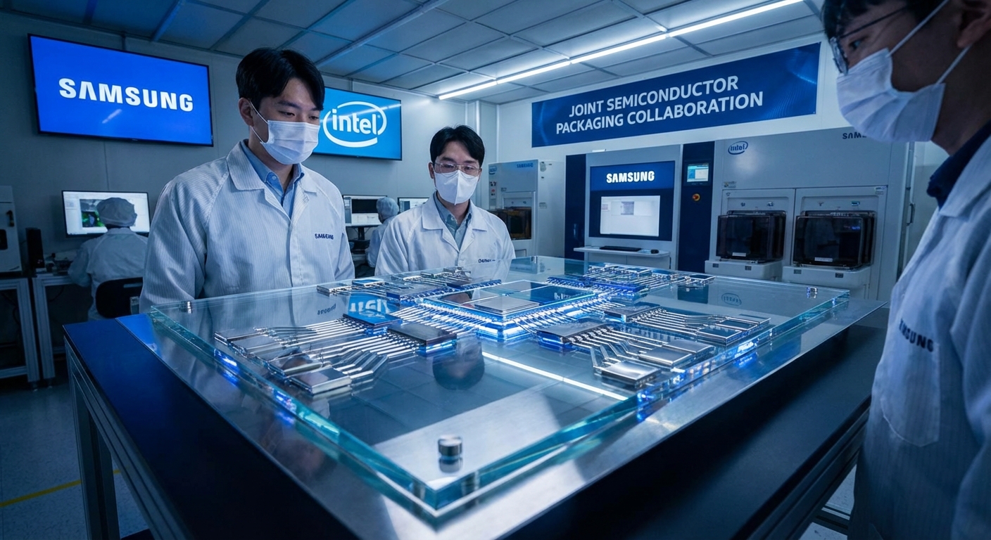
AMD Zen 7 'Grimlock' CCDs are slated for TSMC's 1.4nm A14 node with Powertech FOPLP under evaluation, the first credible signal a flagship server CPU may break from TSMC CoWoS in 2028. TrendForce flags warpage control, redistribution-layer lithography and panel-handling as the three engineering questions Powertech must close before A14 silicon rides on fan-out panel carriers — re-rating every OSAT that has treated panel-level packaging as mid-range.
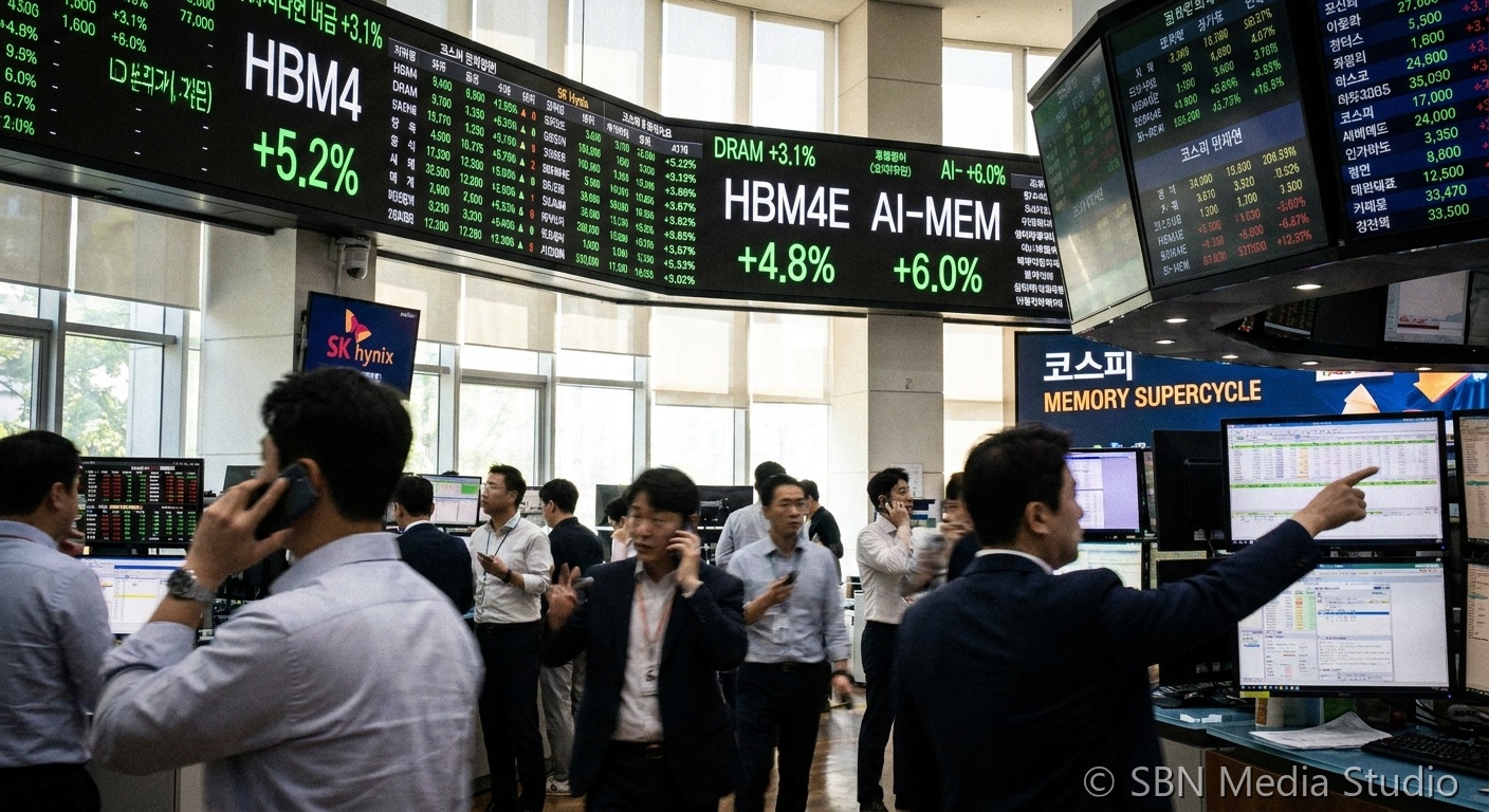
SK Hynix shares hit 1,680,000 won on May 27 — up 186% YTD — as Microsoft, Google and Amazon offer to underwrite HBM capacity expansion. The Korean memory maker now trades on a $230 billion market cap, third-largest in Asia, with a Q1 operating margin of 72% that tops NVIDIA. The AI-memory supercycle has shifted bargaining power from foundry to memory for the first time in a decade.
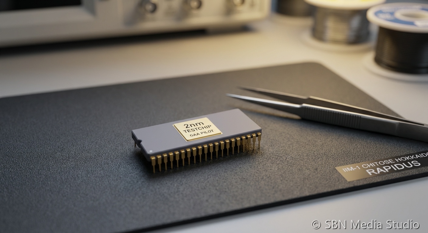
Japan's Rapidus has begun 2nm gate-all-around pilot wafers at IIM-1 Chitose with Canon as its first paying customer and 60+ firms in commercial discussions ahead of a 2027 ramp. Tokyo has anchored an additional ¥167.6 billion in private funding and a $1.7 billion government-private bridge, positioning Rapidus as a credible fourth leading-edge foundry alongside TSMC, Samsung and Intel — the Asia-Pacific story heading into Computex week.
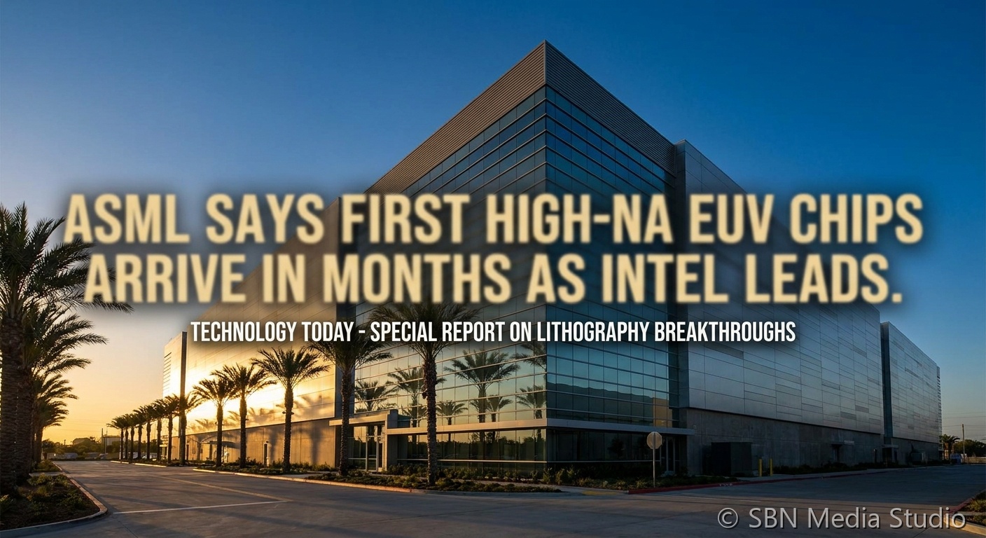
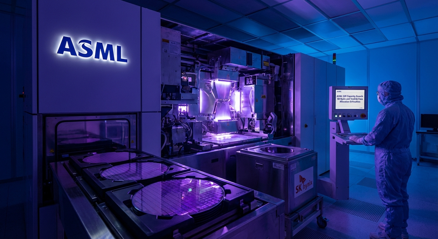
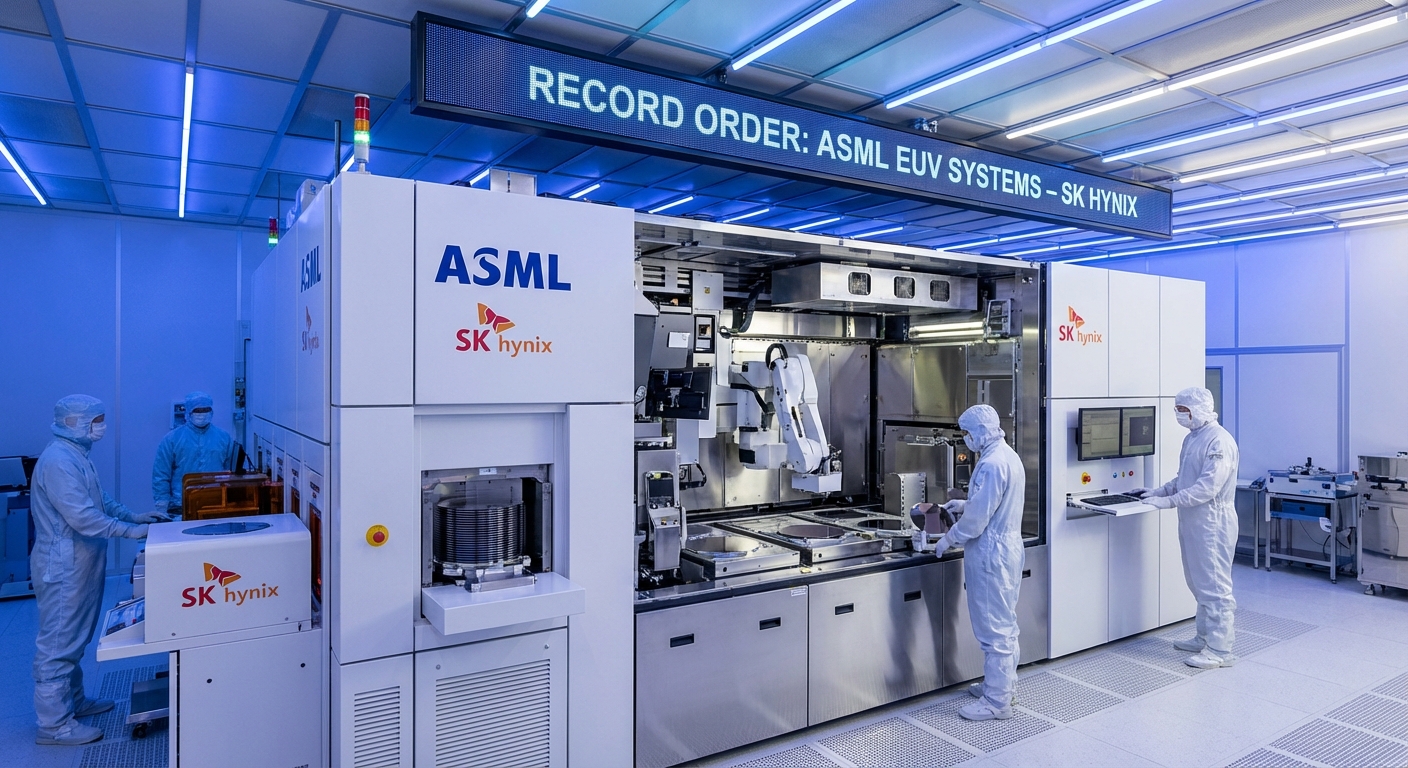
ASML CEO Christophe Fouquet told the imec Future Summit on May 19 that the first commercial chips produced on the $400M-per-tool High-NA EUV platform will surface in months across both memory and logic. Intel already has two systems running and has exposed 300,000 wafers; SK Hynix is anchoring an $8B order for HBM and DRAM. TSMC has deferred High-NA for A14/A13 as too expensive, splitting the industry.
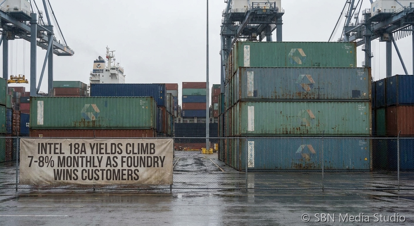
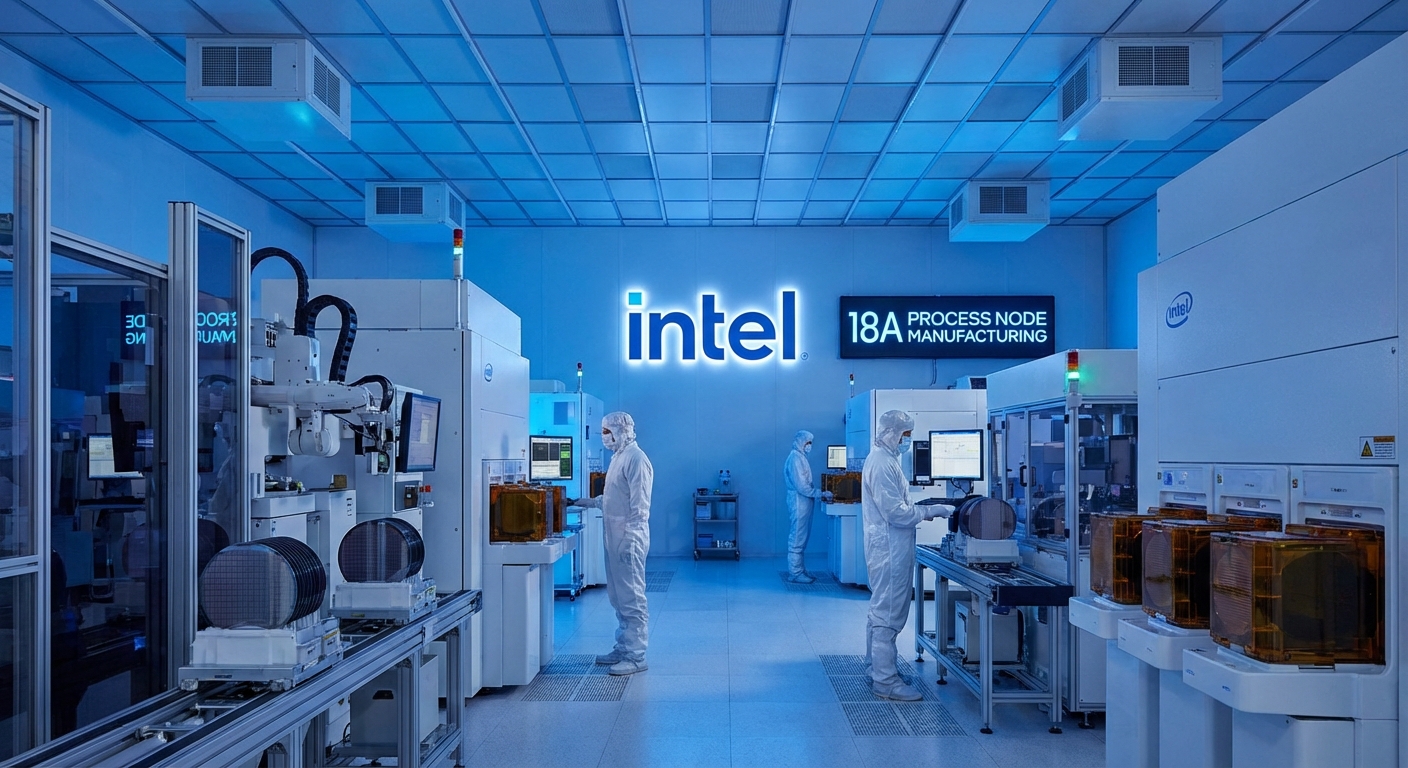
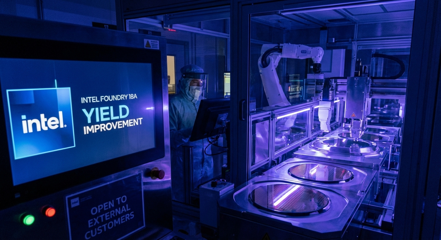
CEO Lip-Bu Tan told CNBC on May 18 that 18A yields are improving 7–8% per month — best-practice pace — and that Intel expects commitments from multiple external foundry customers in H2 2026. Microsoft's Maia 2 is slated for 18A; NVIDIA is exploring putting the I/O die of its 2028 Feynman GPU on 18A or 14A with EMIB packaging; Apple already has the 18A-P PDK in simulation.
TSMC told its Hsinchu symposium on May 14 that CoWoS yields are now above 98% and combined CoWoS/SoIC capacity will roughly double again this year across 18 new fabs and packaging facilities. The roadmap now includes a 14-reticle CoWoS package with 20 HBM stacks in 2028 and a 24-HBM beyond-14-reticle platform in 2029 — targeting a 48x leap in package-level compute.
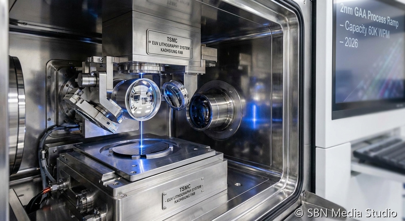
Five TSMC 2nm fabs are entering volume ramp this year — the most aggressive node expansion in the company's history. Supply-chain trackers estimate monthly N2 capacity will pass 60,000 wafers in 2026 and approach 140,000 by year-end, a 45% lift over peak 3nm output. Apple, NVIDIA and AMD have already pre-booked the slots, leaving little slack for new entrants.
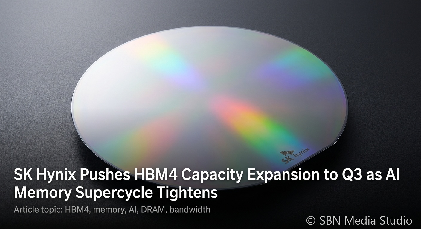
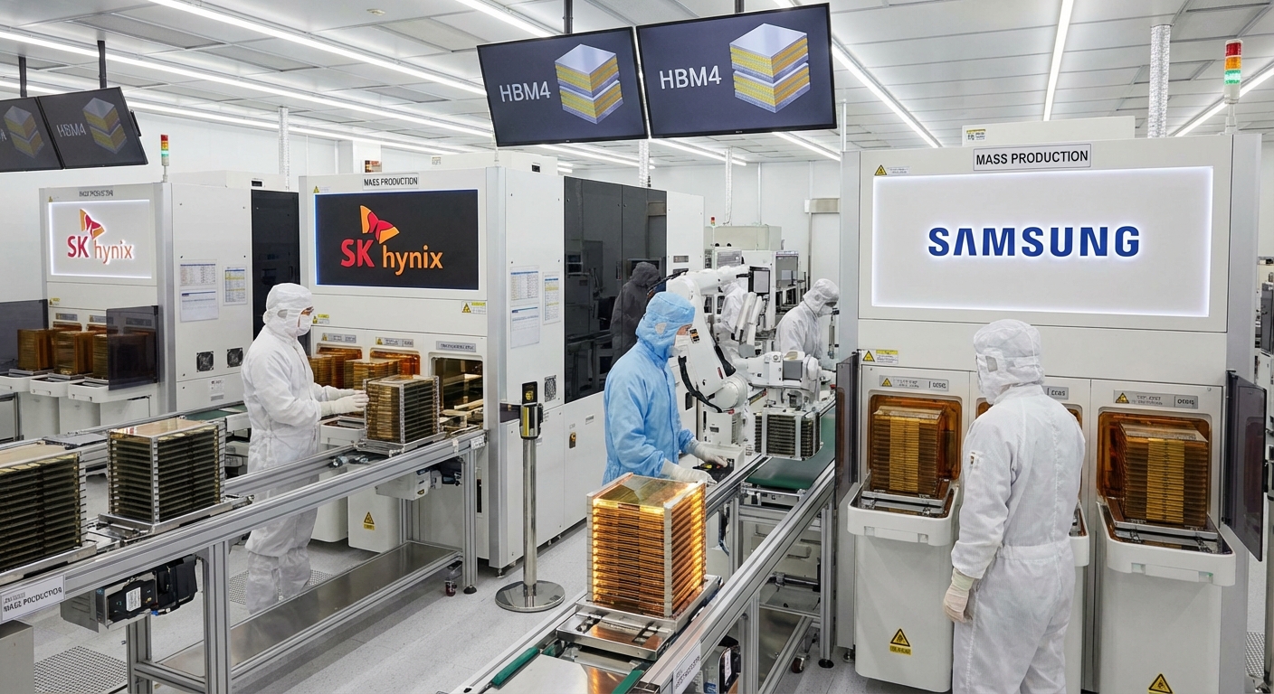
SK Hynix has slipped the second leg of its HBM4 capacity build-out from Q2 to Q3 2026, even as its world-first HBM4 mass production kicked off in February at M16 Icheon and M15X Cheongju. The 12-Hi stacks pair a TSMC 12nm logic base die with 2,048-bit I/O, doubling bandwidth and lifting power efficiency over 40%. SK Hynix, Samsung and Micron are now all chasing NVIDIA's expanded 16-Hi HBM4 orders for Vera Rubin.
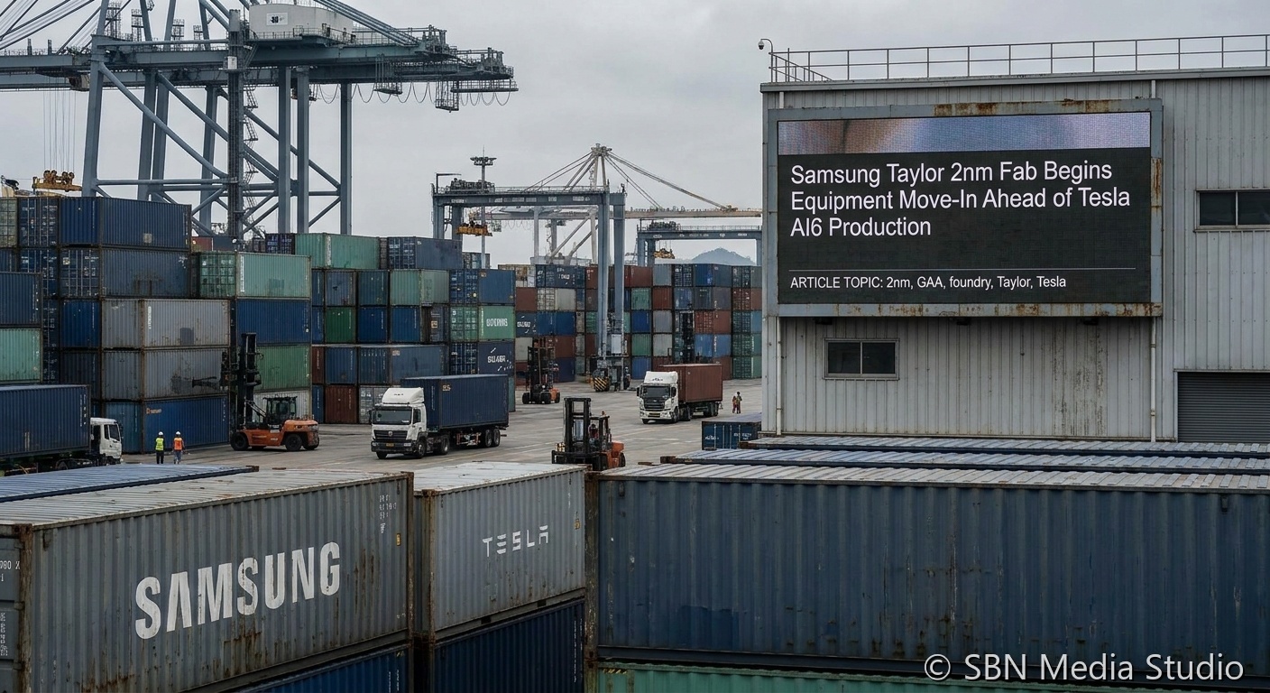
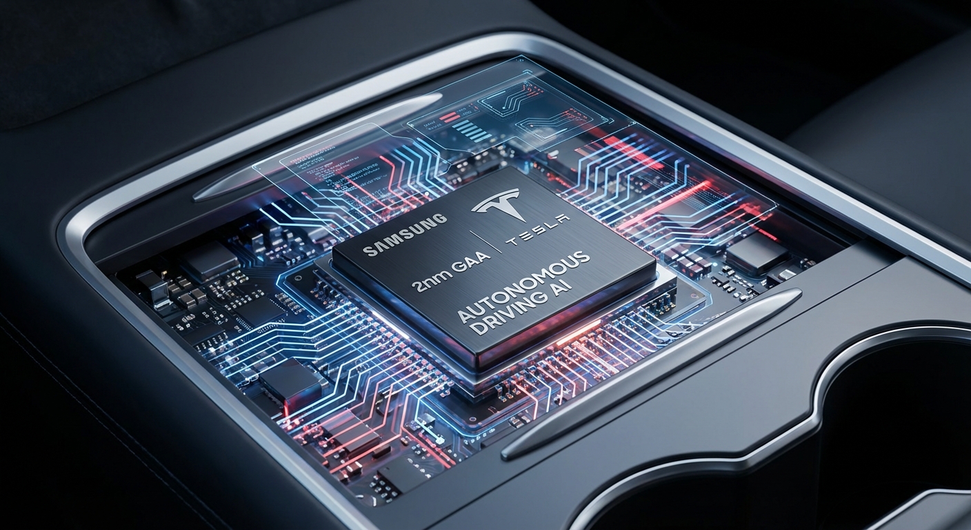
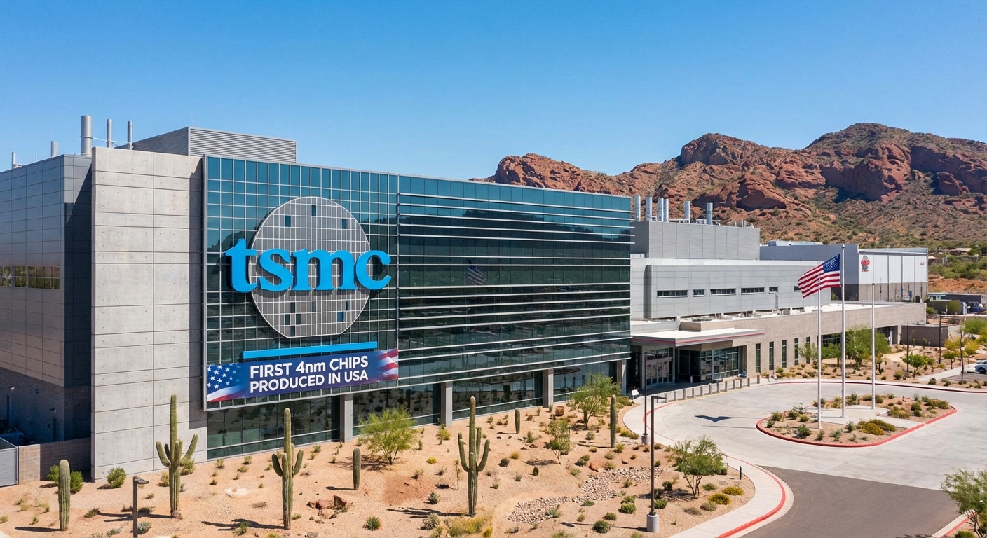
Samsung Foundry has begun installing lithography tools at its $37 billion Taylor, Texas plant, putting the long-delayed 2nm GAA line on track for second-half 2026 first silicon. The fab anchors a $16.5 billion contract to produce Tesla's AI6 autonomous-driving chip — though Tesla's AI6 ramp has slipped roughly six months on Samsung yield issues. Samsung is splitting Tesla's silicon with TSMC Arizona, which will handle the optimized AI6.5 variant.
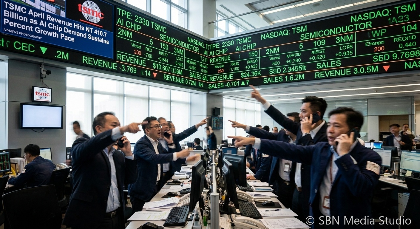
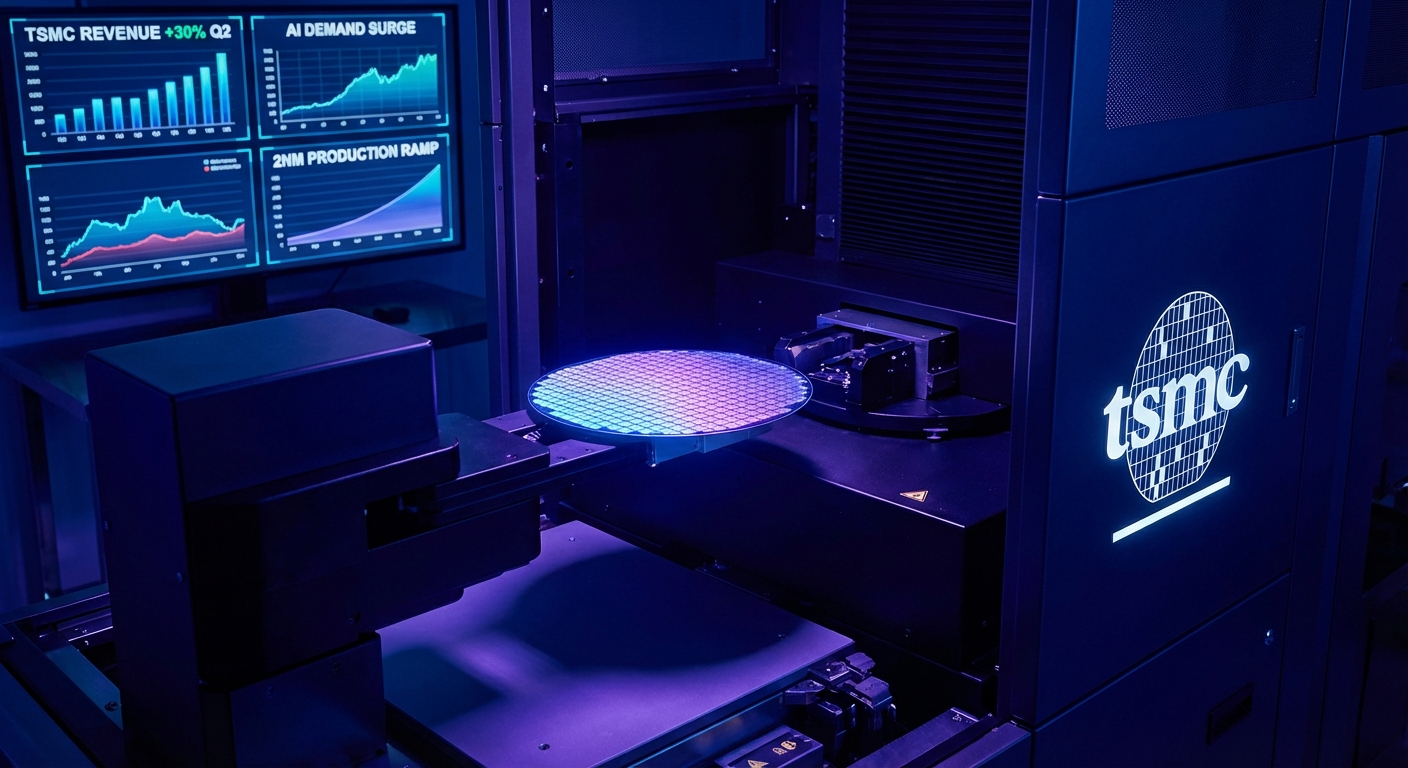
TSMC reported April 2026 monthly revenue of NT$410.726 billion, up 17.5% year-over-year, with cumulative four-month revenue approaching NT$1.55 trillion. The data keeps the foundry tracking ahead of its raised full-year 2026 guidance of more than 30% USD growth, with AI accelerators continuing to consume the bulk of leading-edge capacity.
Apple and Intel have reached a preliminary agreement for Intel to manufacture some of Apple’s future chips, the Wall Street Journal reported on May 8. Intel stock jumped as much as 19% on the news, the most material external foundry customer win since Lip-Bu Tan became CEO. The deal would dent Apple’s decade-plus reliance on TSMC for leading-edge silicon.
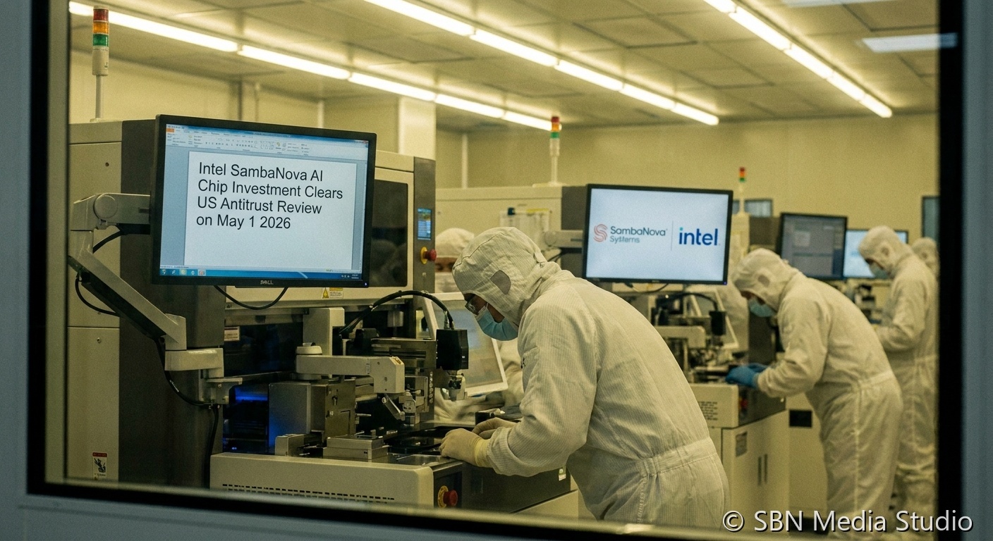
U.S. antitrust regulators on May 1 closed early-termination on Intel’s investment in SambaNova, the AI inference chip startup chaired by CEO Lip-Bu Tan. Intel has put $35M in already plus a planned $15M add-on, lifting its stake to 8.2%. The first co-designed Xeon-6 + RDU inference system targets H2 2026.
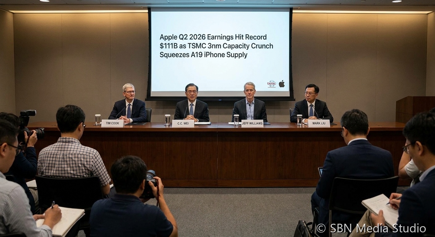
Apple on April 30 reported fiscal Q2 revenue of $111.2B (+17% YoY) and Services at a record $30.98B, but Tim Cook flagged that iPhone 17 unit volume was capped by supply, not demand. The bottleneck is TSMC’s 3nm and 2nm capacity, which is now prioritized for AI accelerators from NVIDIA, AMD and Broadcom. Apple guided that the silicon shortage is unlikely to ease before fiscal 2027.
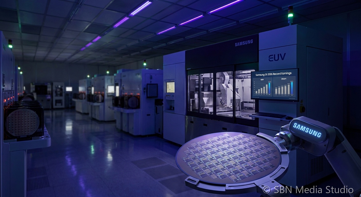
Samsung Electronics reported on April 30 that Q1 2026 operating profit surged more than eightfold year-over-year to 57.2 trillion won (~$41.8B) on revenue of 133.9 trillion won, both record highs. The Device Solutions chip division accounted for over 90% of group profit, with management noting that conventional DRAM is currently more profitable than HBM because DRAM contracts price quarterly while HBM is locked annually.
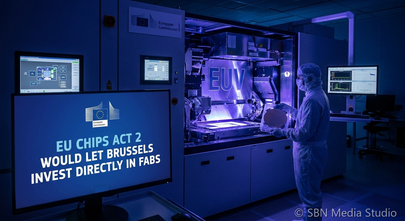
A draft of the European Commission's revamped Chips Act, expected in late May, would for the first time allow the bloc's executive arm to take direct equity stakes in semiconductor fabs on European soil, Bloomberg reported on April 30. The proposal is meant to compete with U.S. CHIPS Act funding and Asian state support, after the original 2023 Chips Act was widely criticized for relying solely on member-state subsidies.
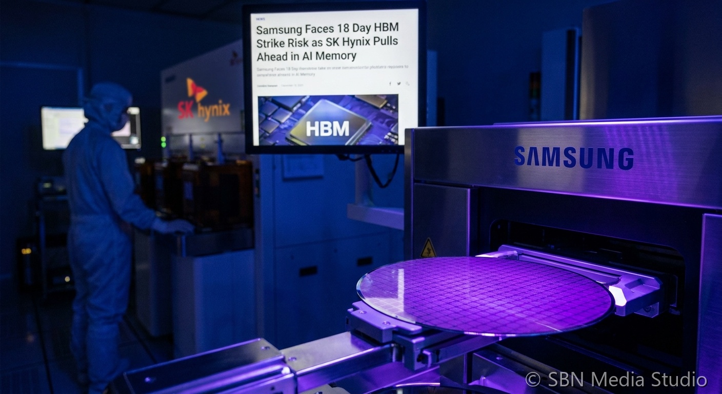
Samsung Electronics' national union has announced an 18-day general strike from May 21 to June 7 over performance-based bonuses, with industry observers warning the action could disrupt high-bandwidth memory production and customer engagement at the worst possible moment. SK Hynix continues to consolidate its HBM3E lead while sampling HBM4 to key customers, and analysts cited by UPI and Seoul Economic Daily peg potential losses at up to 30 trillion won (€17.34B) if the strike proceeds as planned.
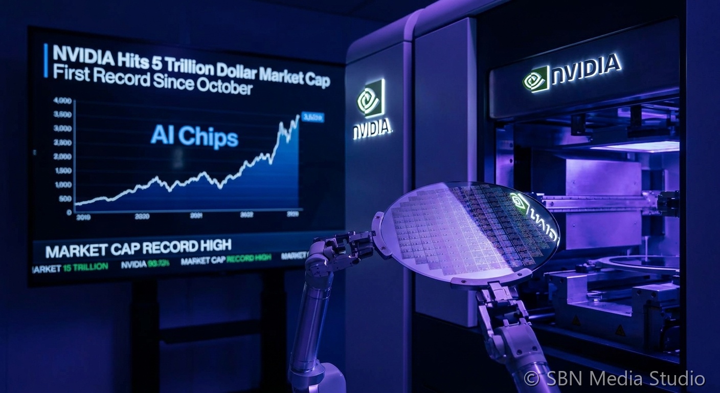
NVIDIA shares rose 4.3% to close at $208.27 on Friday, April 24, taking the company's market capitalization past $5 trillion and notching its first record close since October 2025. The rally was sparked by Intel's blowout Q1 earnings the night before and broader bullishness on AI chip demand ahead of NVIDIA's own fiscal Q1 results on May 20, where management has guided revenue of $78 billion ±2%.
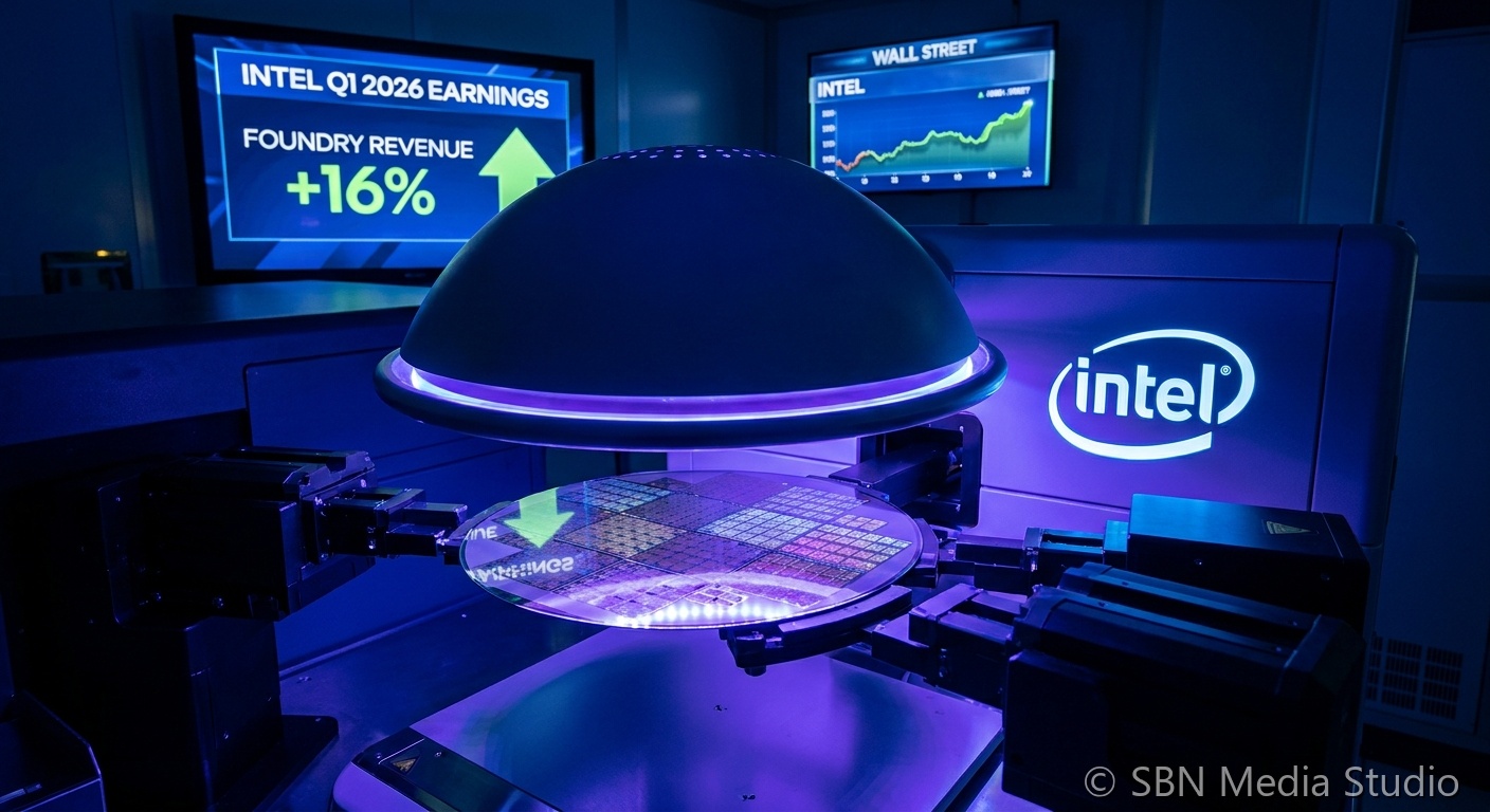
Intel reported Q1 2026 revenue of $13.6 billion versus the $12.42 billion consensus, with EPS of $0.29 against a $0.01 estimate. Intel Foundry revenue rose 16% year-over-year to $5.4 billion, and shares closed up roughly 24% at $82.57 on April 24 — the company's largest single-day gain since 1987 — as investors bought the AI-and-foundry turnaround thesis. TrendForce separately reported that Intel's 14A node may attract major external customers by year-end as PDK 1.0 nears.
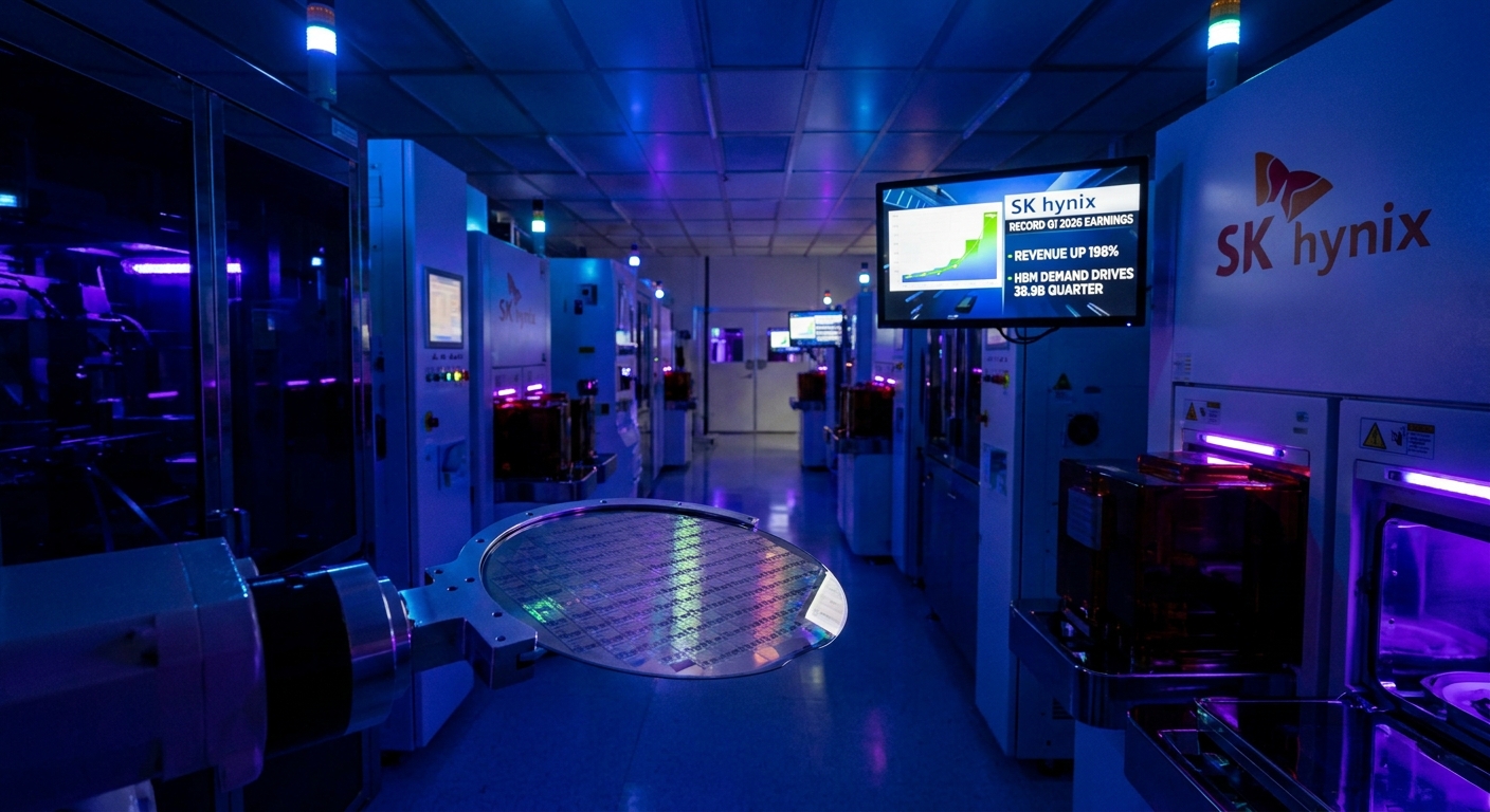
SK Hynix reported first-quarter 2026 revenue of 52.58 trillion won ($38.9 billion), up 198% year-over-year, with an all-time high operating margin of 72% and operating profit of 37.61 trillion won ($27.8 billion). The company attributed the record results to surging AI infrastructure demand and rising memory prices, and confirmed plans to supply HBM4E samples in the second half of 2026 ahead of mass production targeted for 2027.
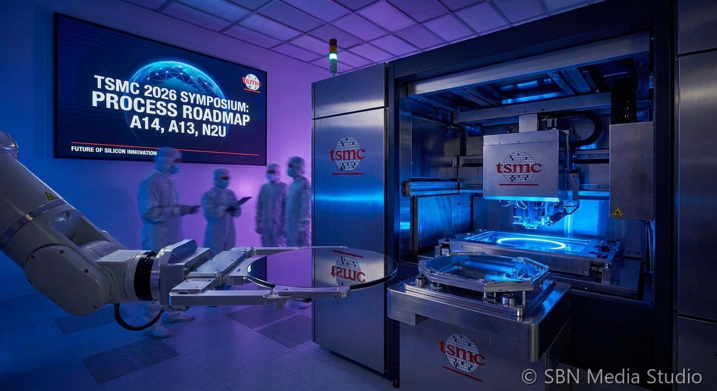
At its 2026 North America Technology Symposium in San Jose, TSMC introduced three new fabrication processes: A14 with NanoFlex Pro for 2028, a 1.3 nm-class A13 node for 2029, and N2U as an extension of the N2 family targeted for 2028. Tom's Hardware and Semiconductor Engineering reported that A16 high-volume production was pushed to 2027, while TSMC also approved 900 acres of new Arizona land for advanced packaging and 3D-IC capacity.
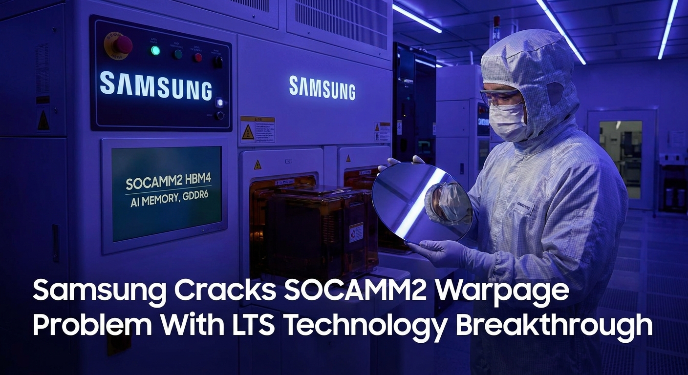
Samsung has reportedly resolved the warpage defect plaguing its SOCAMM2 AI server memory module using internally developed low-temperature solder (LTS) technology, potentially gaining a mass production timeline edge over SK Hynix and Micron. Separately, Samsung is ramping GDDR6 production specifically for Tesla's Dojo supercomputer from April 2026 while scaling back its broader 1d DRAM mass production plan. The moves signal a deliberate pivot toward high-value AI memory partnerships after Samsung ceded HBM market share to SK Hynix in the prior cycle.
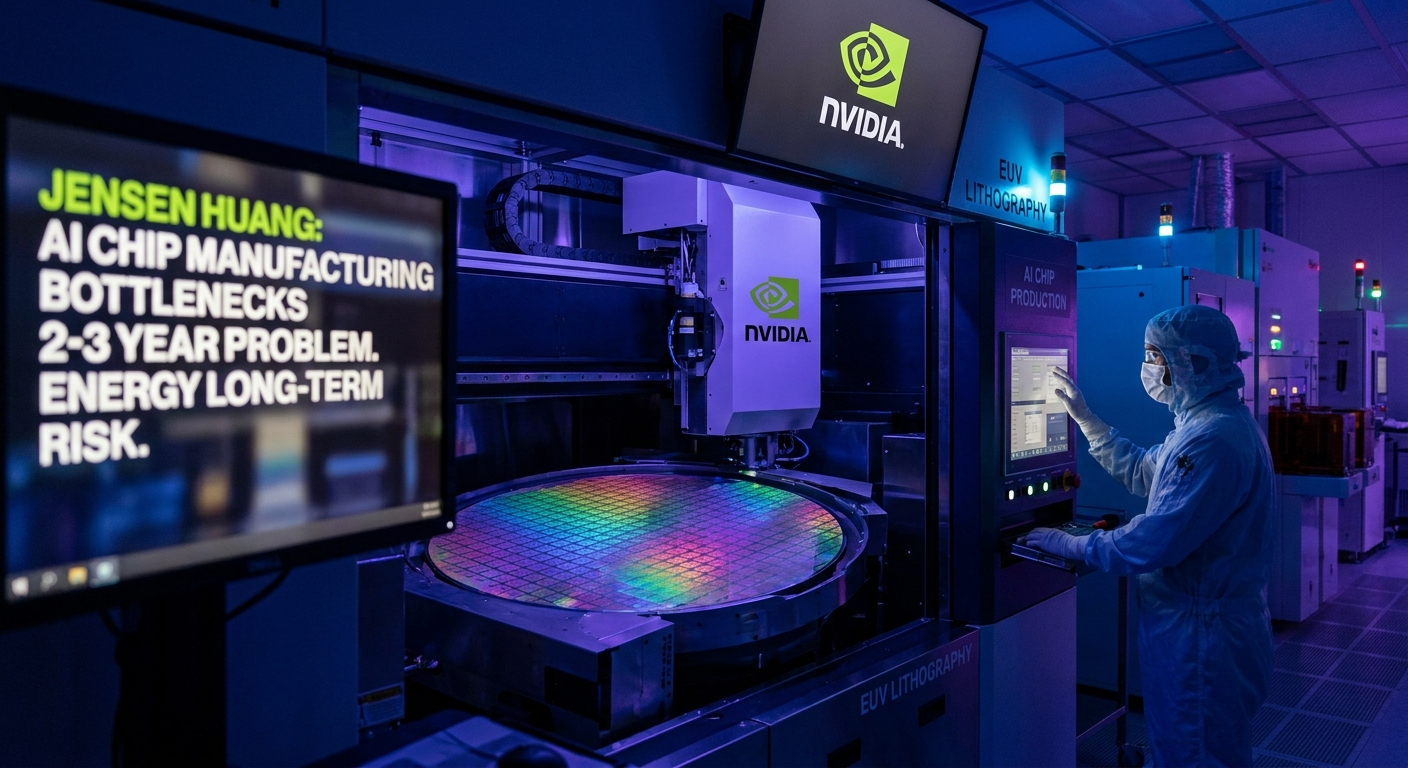
In a wide-ranging podcast interview, NVIDIA CEO Jensen Huang said every bottleneck in advanced packaging, EUV lithography, and memory — including CoWoS capacity constraints — gets solved within two to three years once the demand signal is clear. Huang warned, however, that energy policy and grid capacity represent the legitimate long-term constraint for AI infrastructure build-out, a factor beyond any single company's control.
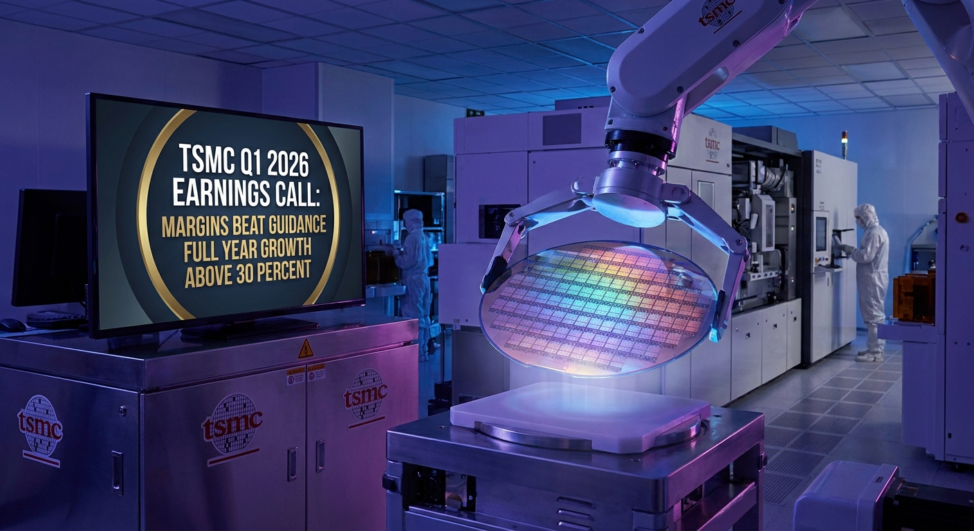
TSMC's formal Q1 2026 earnings call on April 16 confirmed gross margin of 66.2% and operating margin of 58.1% — both exceeding the guided range by several percentage points. CEO C.C. Wei upgraded the full-year growth forecast to "above 30%" in U.S. dollar terms and confirmed CoWoS advanced packaging capacity will reach 130,000 wafers per month by late 2026 to meet surging demand from AI chipmakers including Nvidia.
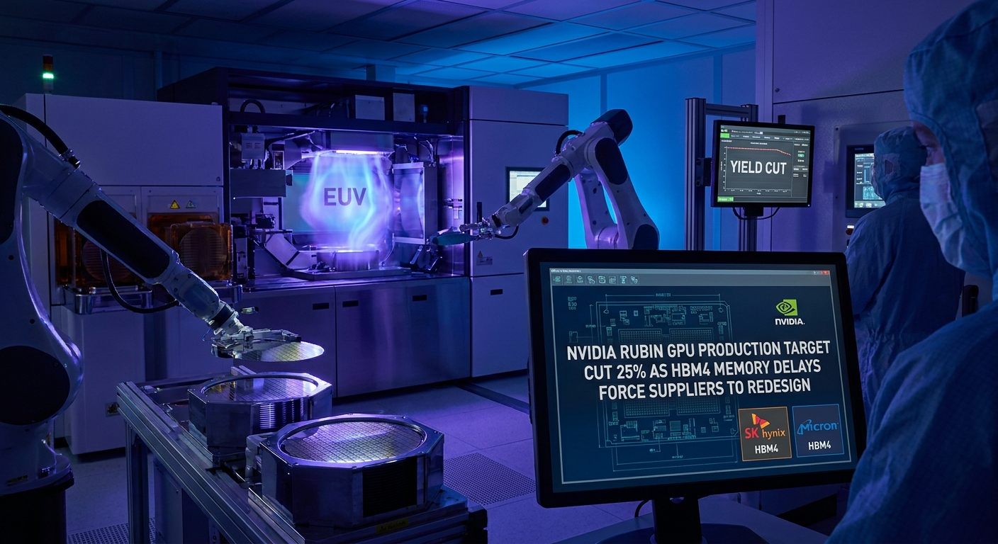
NVIDIA has lowered its 2026 Rubin GPU production target from 2 million to 1.5 million units after SK Hynix and Micron were forced to redesign HBM4 products to meet revised specifications, pushing mass manufacturing back by at least one quarter. SK Hynix is also reportedly weighing a 20–30% cut to planned 2026 HBM4 shipments. Industry analysts now expect Rubin to account for 22% of NVIDIA's high-end GPU mix in 2026, down from a prior forecast of 29%.
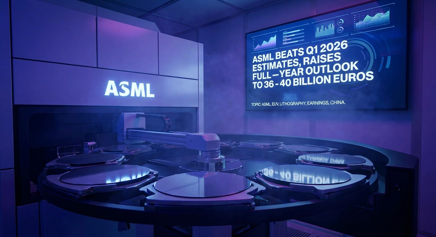
ASML reported Q1 2026 net sales of €8.8 billion and net income of €2.8 billion, both beating analyst forecasts. The Dutch chip equipment maker raised its 2026 full-year sales guidance to €36–40 billion from €34–39 billion, driven by surging AI-related EUV demand. Shares fell 6% as investors focused on tightening China export restrictions expected to reduce the country's share of total sales.
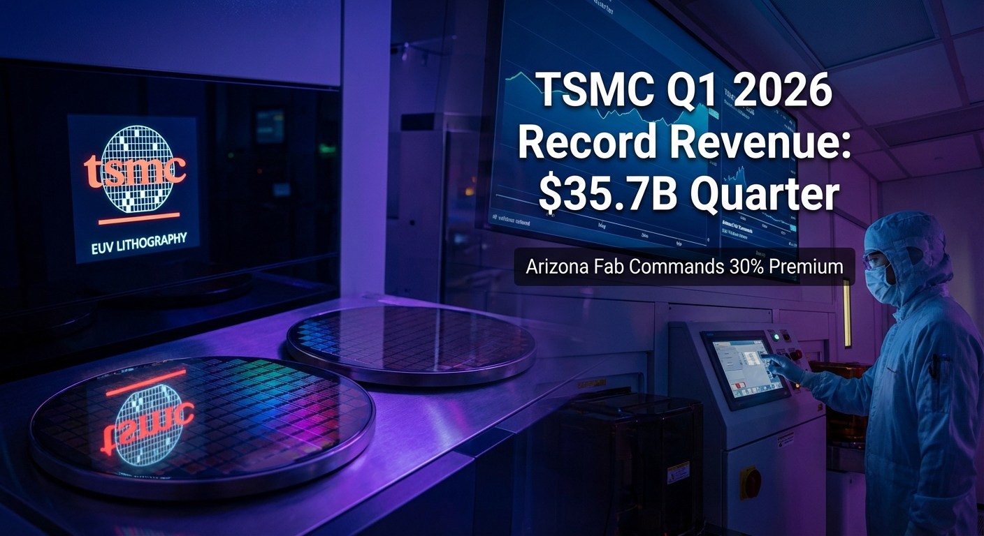
TSMC reported first-quarter 2026 revenue of $35.7 billion — a 35% year-on-year jump and the first time the company has ever surpassed the NT$1 trillion threshold in a single quarter. Arizona's Fab 4 is fully booked through 2027 and commands a 25–30% price premium over identical Taiwan-made wafers, as customers pay a "resiliency tax" for supply chain security ahead of the formal Q1 earnings call on April 16.
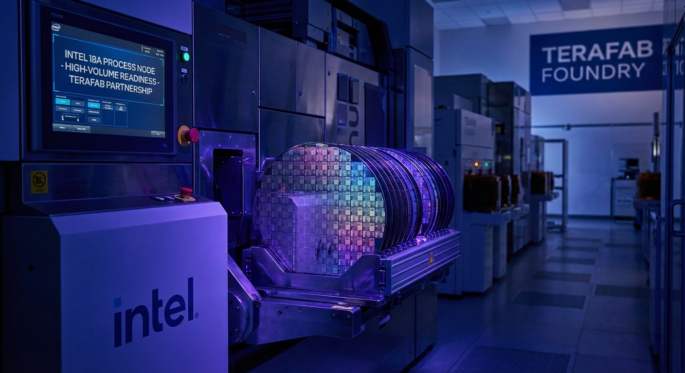
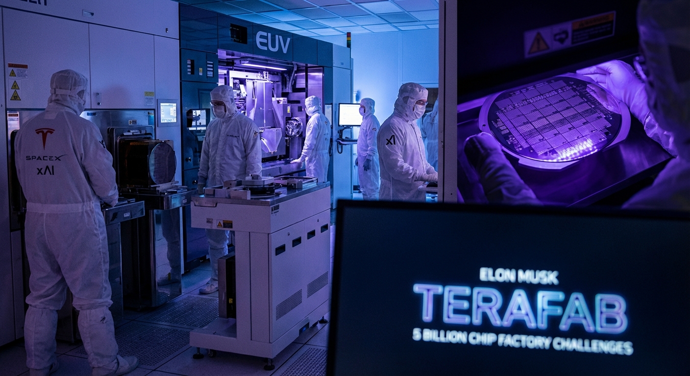
Intel confirmed its 18A (1.8nm-class) process node is now high-volume ready — completing its "5 nodes in 4 years" recovery program — while simultaneously joining Elon Musk's $25 billion Terafab project as primary foundry partner, targeting one terawatt per year of AI compute for Tesla, SpaceX, and xAI. Intel's market cap crossed $300 billion for the first time in 25 years on the combined news.
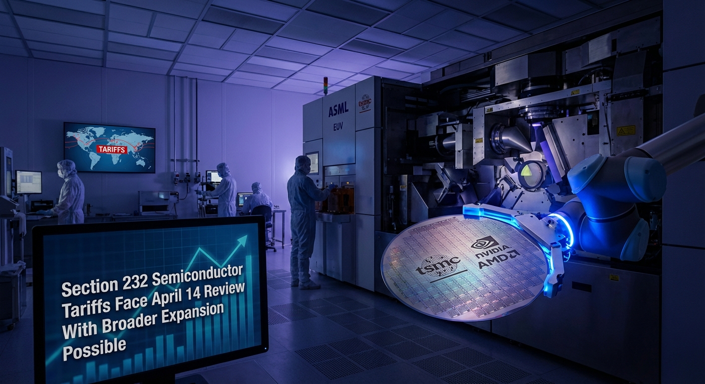
The 90-day window from President Trump's January 2026 Section 232 chip proclamation expired on April 14, 2026, clearing the path for broader tariffs on semiconductors, manufacturing equipment, and derivative products across the entire supply chain. Commerce Secretary Howard Lutnick delivered the required trade negotiation report to the White House, and the industry is now bracing for a second, wider tariff proclamation that could reshape chip pricing globally.
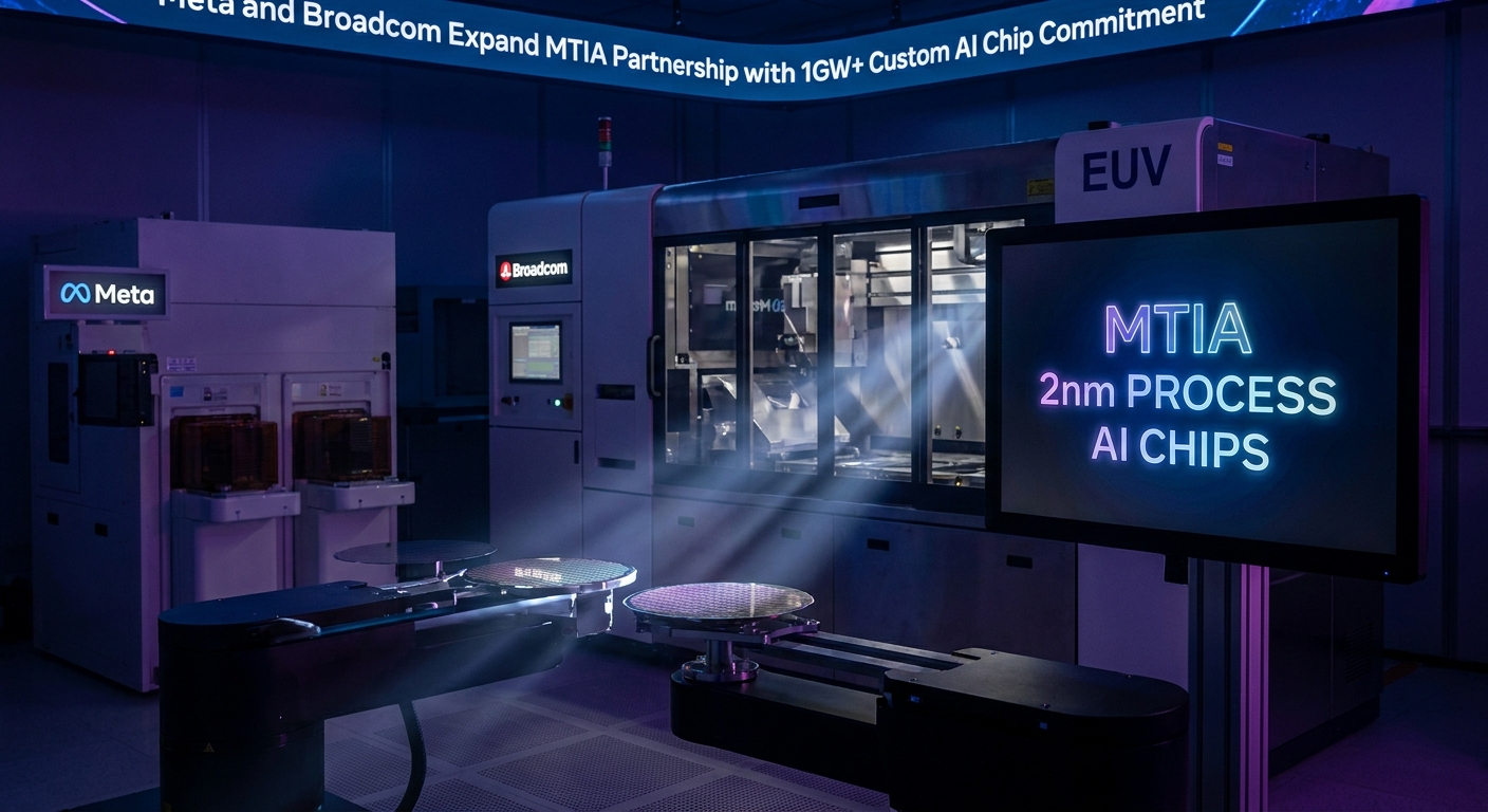
Meta and Broadcom extended their custom silicon partnership through 2029, committing to co-develop four generations of Meta's MTIA AI accelerator chip with a first-phase commitment exceeding 1 gigawatt of deployed compute. The MTIA chips will be the first AI silicon to use a 2nm process node, and will power ranking, recommendations, and generative AI across Meta's apps and services. Broadcom CEO Hock Tan will transition off Meta's board to an advisory role as part of the agreement.
South Korean semiconductor exports surged 152% year-over-year to a record $8.6 billion in the first 10 days of April 2026, the highest amount ever recorded for an opening period of any month. Chips now represent 34% of all South Korean exports — up from 18.4% a year earlier — driven by AI infrastructure demand fueling Samsung and SK Hynix's HBM and DRAM shipments globally.
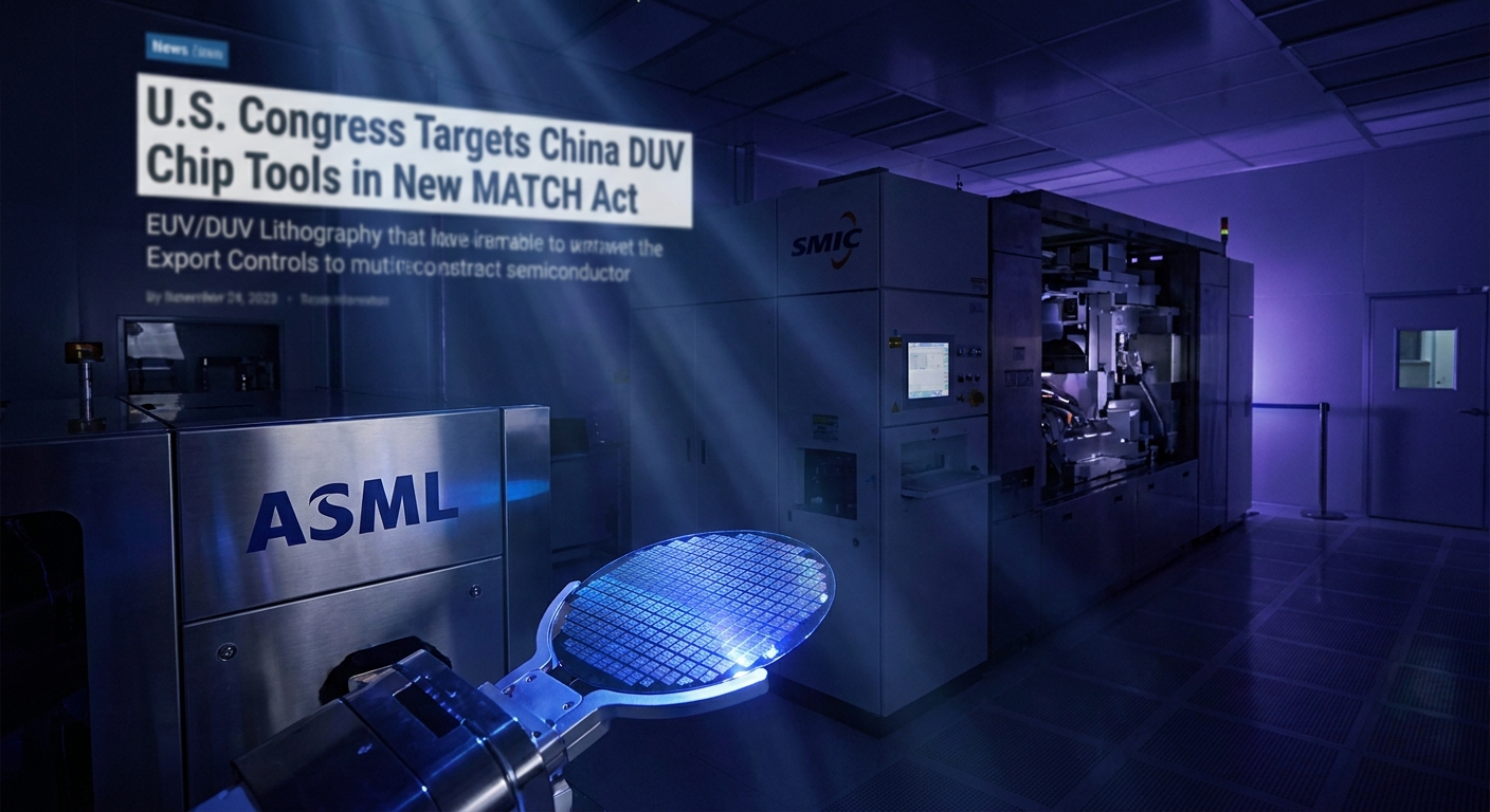
Bipartisan U.S. lawmakers introduced the MATCH Act on April 2, 2026, proposing to ban exports of ASML deep ultraviolet (DUV) immersion lithography systems and Tokyo Electron cryogenic etching tools to China — closing a loophole that has let SMIC and Hua Hong continue building less-advanced chips. The bill would also restrict maintenance and technical support on existing DUV installations and mandate allied-nation coordination with the Netherlands and Japan. ASML shares fell ~2.6% on the news; the company's China exposure is already forecast to drop from 33% of 2025 sales to approximately 20% in 2026.
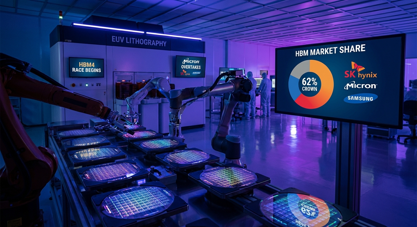
SK Hynix commands 62% of the global HBM market with Micron at 21% and Samsung trailing at 17%, as Micron has officially overtaken Samsung for the second-place position. SK Hynix has also surpassed Samsung as the world's largest DRAM maker by revenue. With HBM3E supply allocated, competition is now pivoting sharply to HBM4, where all three memory giants are racing to qualify with NVIDIA.
TrendForce reported on April 9, 2026 that Samsung and SK Hynix are abandoning annual DRAM and HBM contracts with major hyperscalers in favor of 3-to-5-year long-term agreements. SK Hynix is in advanced talks with Google on a five-year commodity DRAM deal — potentially extending to seven years with HBM conditions — and is finalizing a multi-year DDR5 agreement with Microsoft worth tens of trillions of won as HBM4 ramp begins.
Intel announced on April 7–8, 2026 that it is joining Elon Musk's TeraFab initiative alongside Tesla, SpaceX, and xAI, with the stated goal of producing one terawatt per year of compute power for AI and robotics applications. Intel's market cap surpassed $300 billion for the first time in 25 years on the news, though no formal SEC filings accompanied the announcement. Intel says it will contribute its ability to "design, fabricate, and package ultra-high-performance chips at scale."
TSMC's March 2026 consolidated revenue is expected to set another record high, with Q1 guidance of US$34.6–35.8 billion ahead of its April 16 earnings call. NVIDIA has reserved the majority of TSMC's CoWoS-L advanced packaging capacity for its Blackwell GPU line — supply so constrained that TSMC has outsourced portions to ASE and Amkor — while CoWoS capacity grows at roughly 80% CAGR but still fails to keep pace with AI demand.
The Trump administration's 25% Section 232 tariffs on advanced chips enter a mandatory review window on April 14, 2026, with the Commerce Department and USTR required to report on trade negotiations. TSMC has committed $165 billion to US manufacturing in exchange for duty-free import relief, while the outcome could expand tariffs to a wider class of semiconductors within 90 days.
ASML demand has outstripped supply as imec takes delivery of the EXE:5200 High-NA EUV tool for sub-2nm research while SK Hynix ($7.9B committed) and Elon Musk-backed TeraFab face allocation difficulties. ASML reported €32.7 billion in 2025 sales and guides €34–39 billion for 2026, with EUV bookings surging 150% quarter-over-quarter in Q4 2025.
The Commerce Department is preparing tariff exemptions for major US cloud hyperscalers on advanced semiconductors, contingent on investment commitments tied to TSMC's $165B+ US expansion. Samsung and SK Hynix, whose HBM chips are embedded in NVIDIA and AMD AI accelerators, remain exposed to tariff pressure as suppliers typically absorb pain-sharing demands from customers.
TSMC's most advanced process nodes — including 3nm and 2nm — are completely allocated through 2028, creating an industry-wide supply bottleneck. Apple holds over 50% of early 2nm allocation while NVIDIA is projected to surpass Apple as TSMC's largest customer in 2026, generating approximately $33B in revenue. TSMC is responding with a major GigaFab expansion in Arizona.
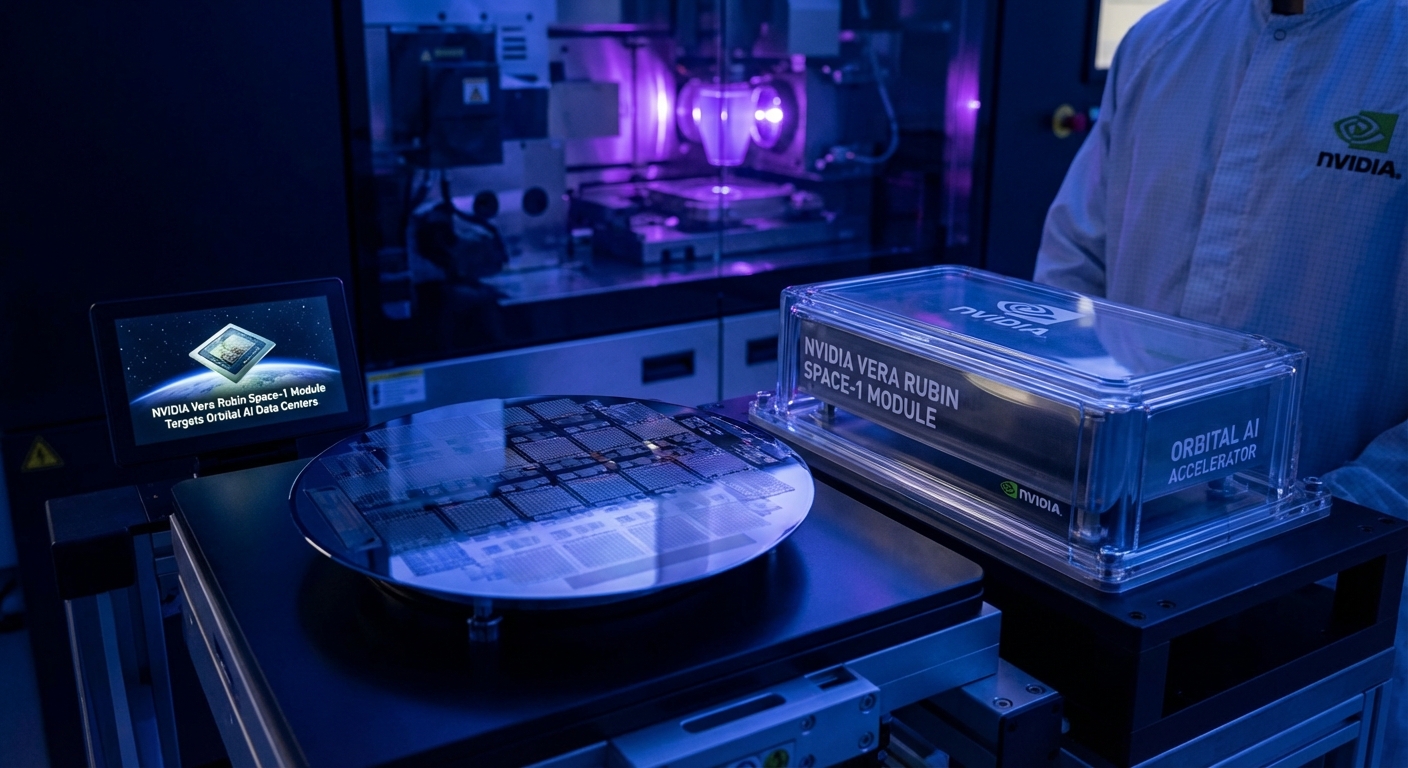
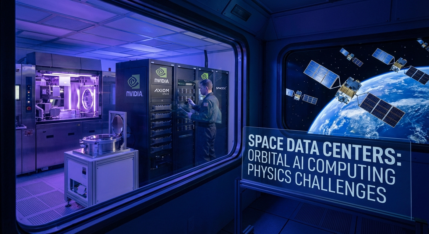
NVIDIA unveiled the Vera Rubin Space-1 Module at GTC 2026, a GPU compute platform designed for orbital data centers claiming up to 25x the AI compute of the H100 in a radiation-hardened form factor. The announcement signals NVIDIA's ambition to extend its AI infrastructure dominance beyond terrestrial hyperscalers into the emerging space computing market. Partners including Axiom Space and Starlab have expressed interest in the platform for low-Earth orbit deployment from 2028.
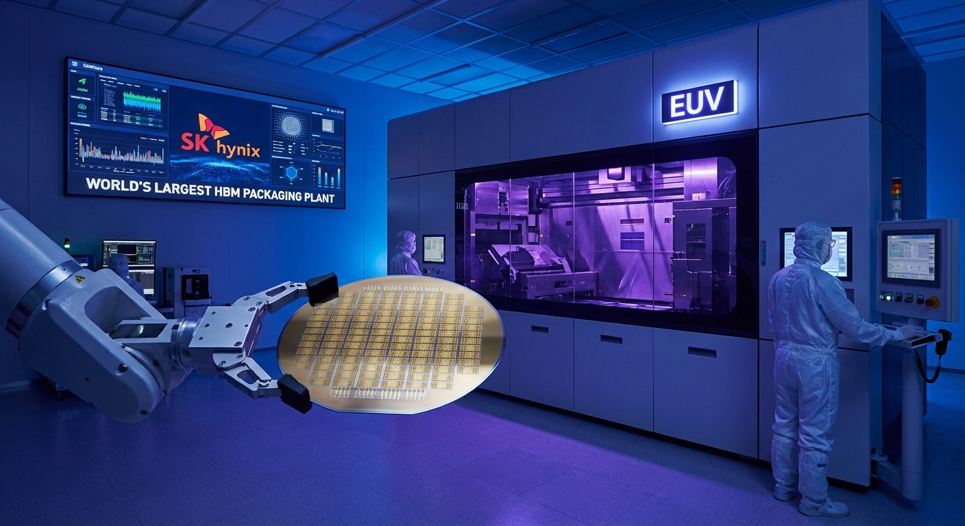
SK Hynix is constructing a massive new advanced packaging facility in Cheongju, South Korea, with a $12.9 billion investment targeting full operations by end of 2027. The P&T7 plant will be the world's largest HBM assembly and test facility, spanning 231,000 square meters and using 2.5D packaging with through-silicon vias to meet surging AI memory demand. SK Hynix projects HBM demand to grow at a 33% CAGR from 2025 to 2030, driven by orders from NVIDIA, AMD, and AI hyperscalers.
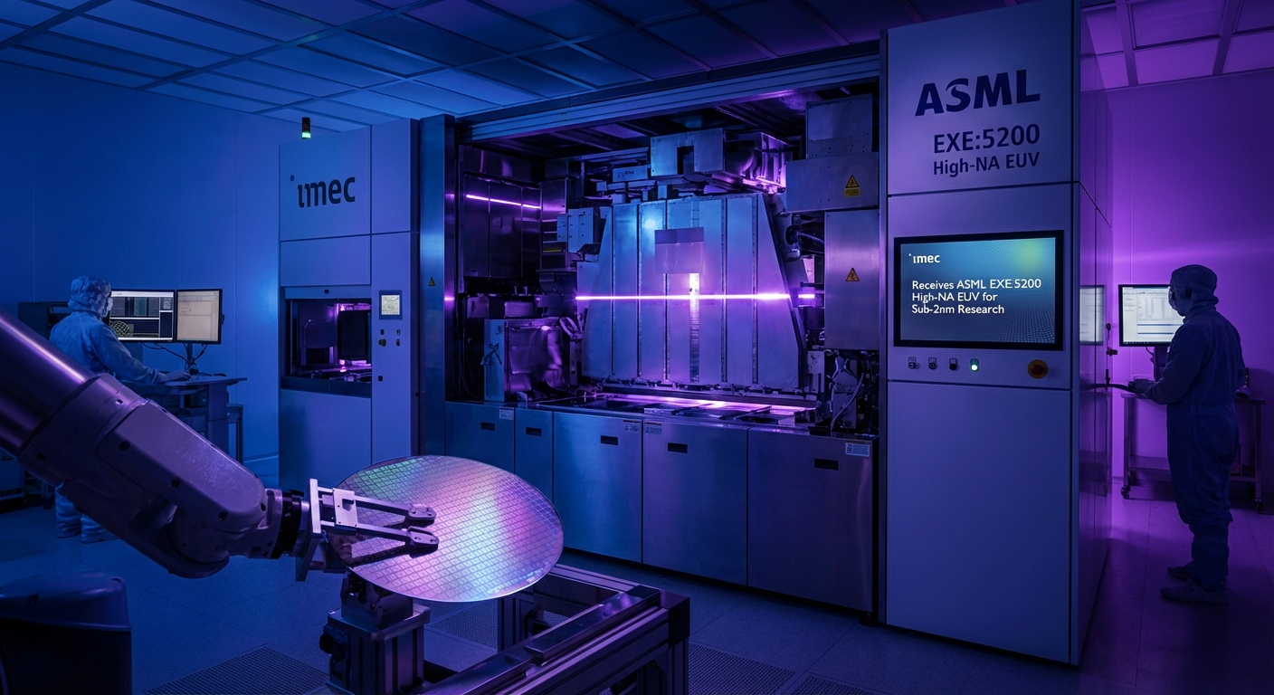
Belgian research institute imec has taken delivery of ASML's Twinscan EXE:5200, a $400 million High-NA EUV lithography system and one of fewer than a dozen units worldwide, with sub-2nm qualification targeted for Q4 2026. The tool features 0.55 numerical aperture optics capable of printing 8nm resolution features in a single exposure — more than doubling the resolution of conventional Low-NA EUV — and achieves 0.7nm overlay performance. Once qualified, the system will open to imec's global partner ecosystem for next-generation logic and DRAM research ahead of expected industry-wide High-NA HVM in 2027-2028.
SpaceX filed to launch one million orbital AI data center satellites. But the physics challenges are staggering: cooling in vacuum requires 1,200 m² radiators per megawatt, radiation causes chip-killing bit flips, and latency limits rule out AI training. A $39B market by 2035 — with RKLB, RDW, BKSY, NVDA, MCHP, and pre-IPO SpaceX as the key plays. Full breakdown of physics, electronics, stocks, and timeline inside.
|SpaceNews, Scientific American, CNBC, Goldman Sachs, EE Times, DatacenterDynamics
Musk announced Terafab on March 21, 2026 — a joint Tesla/SpaceX/xAI venture targeting 2nm chips and one terawatt of AI compute. But with zero semiconductor manufacturing experience, the challenges are staggering: $28B per fab, 38-month build times, ASML equipment backlogs, 60,000 unfilled chip jobs in the U.S., and yields that take years to optimize. Even NVIDIA's Jensen Huang warned it's "virtually impossible" to match TSMC. This deep analysis examines every obstacle Musk must overcome.
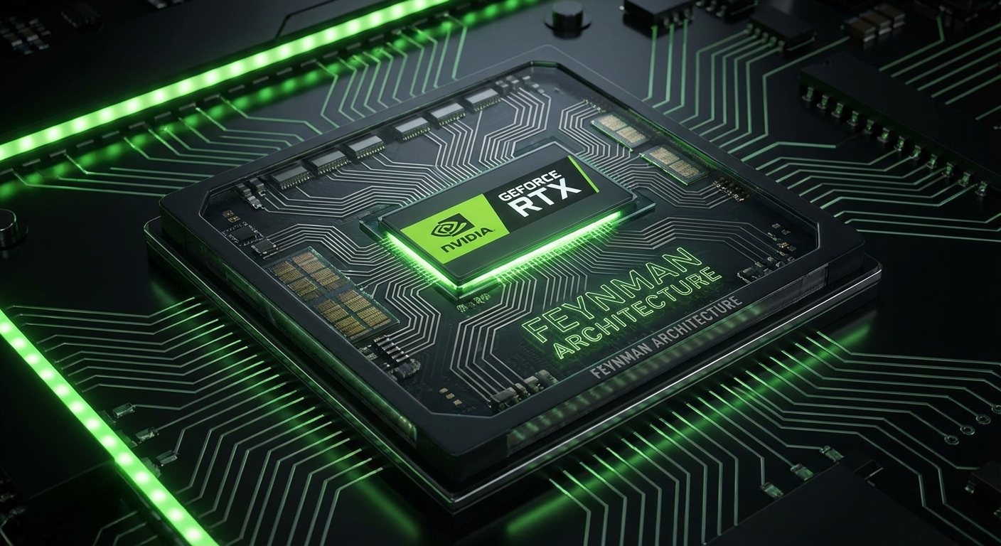
NVIDIA's next-generation Feynman GPU architecture is being designed on TSMC's A16 process node, the foundry's most advanced technology featuring backside power delivery for improved transistor performance and power efficiency. The A16 node represents a generational leap beyond N2, with TSMC claiming 8-10% performance gains and 15-20% power reduction compared to its already-impressive 2nm technology. Feynman is expected to succeed the Rubin architecture and target the data center AI market in 2028, with a transistor count rumored to exceed 400 billion in its flagship configuration — a staggering figure that underscores the relentless pace of GPU scaling driven by AI workload demands.
However, in a significant shift for the NVIDIA chips supply chain, reports indicate the company is also in discussions with Intel Foundry to handle portions of Feynman's chip manufacturing and advanced packaging workloads. The move reflects both the extreme capacity constraints at TSMC and NVIDIA's strategic interest in diversifying its foundry relationships ahead of what is expected to be massive demand for AI-class GPUs in 2027 and beyond. Sources familiar with the discussions say Intel's 14A process node, which incorporates High-NA EUV lithography, is being evaluated for specific chiplets within the Feynman multi-die architecture. Intel's EMIB and Foveros 3D packaging technologies are also under consideration for integrating HBM5 memory stacks with Feynman compute dies.
If confirmed, Intel Foundry would gain its most high-profile external customer to date, potentially validating the Intel 18A and subsequent nodes for the broader semiconductor market. Industry analyst Dylan Patel of SemiAnalysis estimates that even a 15-20% allocation of Feynman production to Intel would represent $3-5 billion in annual foundry revenue — a transformative win for Intel's fledgling external foundry business. The deal would also have significant geopolitical implications, as it would reduce NVIDIA's near-total dependence on Taiwanese manufacturing for its most strategically important products. NVIDIA CEO Jensen Huang has publicly stated that supply chain resilience is a "board-level priority," and the Feynman-Intel discussions appear to be the most concrete manifestation of that strategy to date.
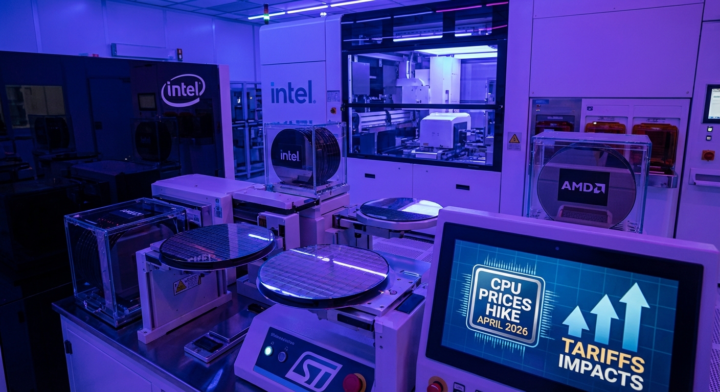
TrendForce reports both Intel and AMD have notified channel partners of 10–15% CPU price increases effective April 2026, citing rising wafer costs, tariff pressures, and tighter leading-edge supply. STMicroelectronics also confirmed broad product line hikes starting April 26, pointing to higher energy, material, and OSAT capacity costs as the period of CPU deflation ends.
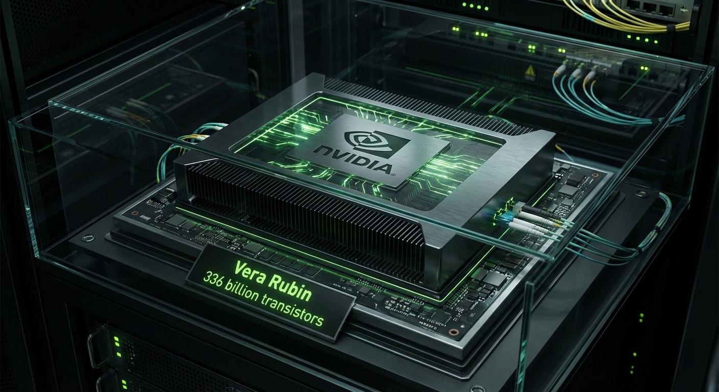
At GTC 2026, NVIDIA CEO Jensen Huang revealed the Vera Rubin platform, the successor to Blackwell, and projected $1 trillion in combined purchase orders for Blackwell and Vera Rubin through 2027 — double the $500 billion projection from just one year ago. The Rubin GPU is built on TSMC's 3nm process with a dual-die design containing 336 billion transistors, delivering 50 PFLOPS of inference compute and 35 PFLOPS for training. The sixth-generation NVLink provides 3.6 TB/s bandwidth per GPU, while the NVL72 rack delivers 260 TB/s — more than the entire internet's bandwidth. AWS, Google Cloud, Microsoft Azure, and CoreWeave are among the first to deploy Vera Rubin systems in H2 2026.
OpenAI, Anthropic, Meta, and xAI have all committed to the Rubin platform, with OpenAI alone reportedly ordering over 100,000 Rubin GPUs for its next-generation training infrastructure. The Rubin platform introduces a fundamentally new memory architecture featuring HBM4 from both SK Hynix and Micron, providing up to 288 GB of HBM per GPU — a 3x increase over Blackwell that enables trillion-parameter models to be loaded entirely in GPU memory without complex model parallelism schemes. Huang also unveiled Kyber, a 144-GPU rack architecture for Rubin Ultra in 2027 that will push rack-level compute to 1.4 exaFLOPS, rivaling today's largest supercomputers in a single rack.
The financial implications are extraordinary. NVIDIA's market capitalization briefly surpassed $5 trillion following the GTC keynote, making it the most valuable company in the world. Wall Street analysts have scrambled to raise price targets, with Bank of America setting a $280 target and citing "unassailable competitive moats in AI silicon." The Vera Rubin platform's 4x energy efficiency improvement over Blackwell is also strategically significant given the Iran conflict's impact on data center energy costs, as hyperscalers can deliver the same compute throughput with substantially lower power consumption. NVIDIA's dominance of the AI accelerator market appears more entrenched than ever, though AMD's MI400 and custom silicon from Google, Amazon, and Microsoft continue to nibble at the edges.
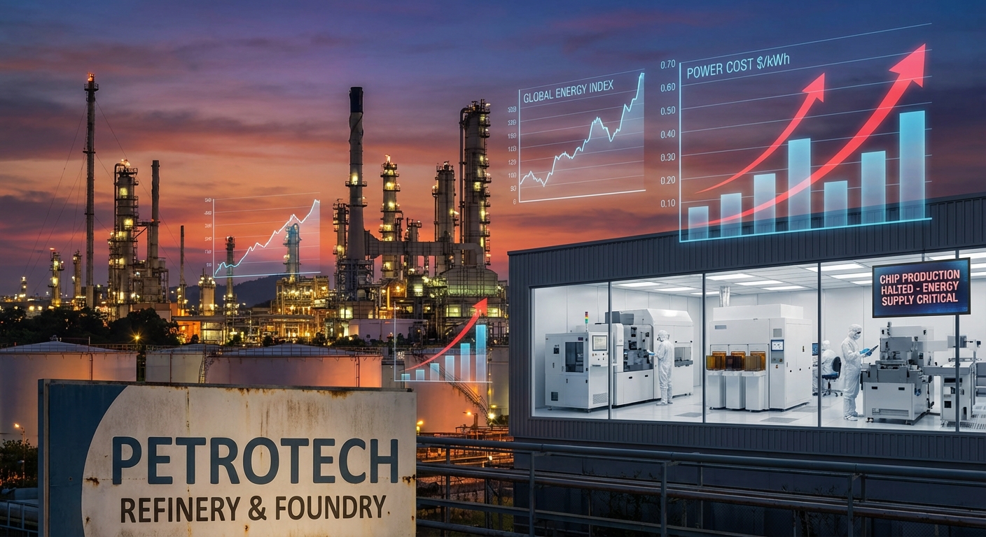
The Iran conflict's most immediate impact on the semiconductor industry is through energy prices. Crude oil surpassing $125 per barrel has triggered a 35% increase in electricity costs across major chip fabrication regions, with South Korea and Taiwan — home to Samsung and TSMC — hit particularly hard due to their heavy reliance on imported energy. A single advanced semiconductor fab consumes roughly 100 megawatts of power continuously, equivalent to a small city, making energy one of the largest variable costs in chip manufacturing. TSMC has warned investors that sustained energy inflation could reduce gross margins by 2-3 percentage points in H2 2026.
Samsung Foundry, already operating on thinner margins than TSMC, faces an even steeper challenge — analysts estimate Samsung's foundry division could swing to an operating loss if energy prices remain elevated through Q4 2026. Intel's U.S.-based fabs benefit from relatively lower energy costs but are not immune, as natural gas prices have risen 28% domestically. The energy shock is accelerating investment in on-site renewable power generation, with TSMC announcing a $2.1 billion solar and battery storage project adjacent to its Kaohsiung facilities.
Industry group SEMI estimates that every $10 increase in oil price adds approximately $800 to the production cost of a single advanced-node wafer. At current oil prices, this translates to roughly $4,000-$5,000 in additional costs per wafer compared to pre-conflict levels, a burden that chipmakers will inevitably pass on to customers through higher pricing. The downstream effects are already visible: major fabless companies including Qualcomm, MediaTek, and Marvell have all flagged potential price increases of 8-15% on next-generation chip orders. Power purchase agreements, once considered routine procurement items, have become boardroom-level strategic discussions at every major semiconductor company.
SK hynix disclosed on March 24 that it has placed the largest single EUV equipment order ever publicly announced, committing approximately 11.9 trillion won ($7.9 billion) for around 30 ASML EUV lithography machines to be delivered by the end of 2027. The machines will support SK hynix's transition to its advanced 1c DRAM node and underpin mass production of HBM4 and LPDDR6 memory for AI workloads. The order dwarfs previous ASML deals in size and signals the intensifying race among DRAM makers to secure lithography capacity before supply of EUV systems tightens further. UBS analysts estimate SK hynix will capture roughly 70% of NVIDIA's HBM4 demand for the upcoming Vera Rubin platform, giving it a commanding lead over Samsung and Micron. The investment reinforces SK hynix's status as the world's most advanced HBM supplier and raises the barrier to entry for competitors seeking to close the gap on next-generation AI memory.
Intel held its annual Foundry Direct Connect event in San Jose on March 24, drawing chipmakers, packaging specialists, and hyperscalers to review its process roadmap. CEO Lip-Bu Tan confirmed that Intel 18A — the flagship process powering the Clearwater Forest server CPU — entered high-volume manufacturing in late 2025 and yields are tracking toward profitability targets by late 2026. The company showcased its Glass Substrate packaging technology and updated its advanced 3D chiplet portfolio, emphasizing differentiated offerings versus TSMC's CoWoS. The critical wildcard remains Intel 14A, the first node to use High-NA EUV lithography. Tan said firm commitments from external foundry customers are expected in the second half of 2026, with Apple reportedly evaluating Intel 14A for select chips in its 2029 silicon roadmap. If a marquee name signs on, it would mark a pivotal validation of Intel's foundry ambitions.
Samsung Foundry has signed a landmark $16.5 billion agreement with Tesla to manufacture AI6 chips on its 2nm GAA process at the Taylor, Texas fabrication facility. The deal represents the single largest foundry contract Samsung has ever secured and validates its aggressive investment in gate-all-around transistor technology. However, production has been pushed back roughly six months, delaying mass production to Q4 2027. Samsung's 2nm yields have reached approximately 50%, with a target of 70% needed to attract further high-profile customers. The Taylor fab has pivoted from its original 4nm plans to focus entirely on 2nm production with an initial capacity of 50,000 wafers per month.
Samsung is targeting 130% growth in 2nm orders for 2026, with Qualcomm, Meta, and Google among potential customers being actively courted. The Tesla AI6 chip is designed for fully autonomous driving applications, requiring a combination of massive neural network inference throughput and automotive-grade reliability that pushes the boundaries of what 2nm technology can deliver. Tesla's decision to consolidate AI6 production with Samsung rather than splitting between Samsung and TSMC (as it did with the AI5 generation) reflects both competitive pricing from Samsung and the strategic advantage of U.S.-based manufacturing under CHIPS Act incentives.
Despite the delay, Samsung's aggressive 2nm push positions it to capture overflow demand from TSMC's fully booked capacity. Industry analysts at TrendForce estimate that Samsung could capture 12-15% of the global 2nm foundry market by 2028, up from its current sub-10% share of advanced nodes. The Tesla contract also provides Samsung with a high-volume "anchor customer" that justifies the enormous capital expenditure required to bring 2nm GAA to mass production — a dynamic similar to how Apple's early commitment to TSMC's leading-edge nodes helped the Taiwanese foundry achieve cost-effective yields years ahead of competitors. Samsung's semiconductor division president, Kyung Kye-hyun, called the Tesla partnership "a defining moment for Samsung Foundry's competitiveness."
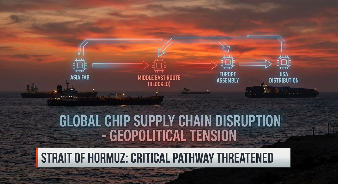
Naval operations near the Strait of Hormuz have forced major shipping carriers to reroute semiconductor raw material shipments around the Cape of Good Hope, adding an average of 18 days to delivery timelines for critical inputs. Neon gas — essential for EUV and DUV lithography processes — has seen spot prices spike 240% as supplies from Middle Eastern refineries face disruption. Palladium, used in chip packaging and multilayer ceramic capacitors, has risen 45% on commodity exchanges. The disruption comes at the worst possible time: TSMC and Samsung are ramping 2nm production, which demands higher volumes of specialty chemicals and ultra-pure materials than any previous node. Logistics firms Maersk and CMA CGM have both issued force majeure notices for Persian Gulf routes, while insurers have raised war-risk premiums for vessels transiting the region by 300%.
Several semiconductor material suppliers, including Shin-Etsu and Air Liquide, are activating contingency stockpiles and exploring airlift options for the most critical components, at costs 8-10x higher than sea freight. Industry insiders report that some chipmakers have only 4-6 weeks of neon gas reserves remaining at current consumption rates, creating an urgent scramble for alternative sources. Ukraine, which supplied roughly 50% of the world's semiconductor-grade neon before the 2022 conflict, has partially restored production capacity, and several U.S. and European suppliers are now fielding emergency procurement requests from TSMC and Samsung. The palladium shortage is particularly acute for advanced packaging processes, where the metal is used in wire bonding and under-bump metallization for flip-chip assemblies. South Africa's Sibanye-Stillwater, the world's largest palladium producer, has reported a threefold increase in spot inquiries from semiconductor customers in the past month alone.
The cascading supply chain disruption extends beyond raw materials to finished semiconductor equipment. ASML has flagged potential 3-4 week delays on delivery of EUV lithography system components sourced from suppliers in the broader Middle East and Indian Ocean shipping corridor. Applied Materials and Lam Research have similarly warned that certain sub-assemblies routed through affected shipping lanes may face delays. The cumulative effect is a supply chain that was already stretched thin by record demand now being tested by a geopolitical shock of a magnitude not seen since the early days of the COVID-19 pandemic. Industry group SEMI estimates that the total logistics cost increase across the semiconductor supply chain could reach $12-18 billion annually if current disruptions persist through the end of 2026.
Samsung has secured an exclusive agreement to supply HBM4 memory for OpenAI's first internally designed AI accelerator, codenamed "Titan." The chip, being built on TSMC's N3 process node, is expected to enter production by end of 2026 and is aimed at dramatically reducing OpenAI's dependence on NVIDIA's GPU ecosystem for inference workloads. Samsung's selection as the sole HBM4 provider is a significant win for its memory division, which has faced stiff competition from SK hynix in the AI memory market. Titan represents OpenAI's broader push — alongside similar efforts at Google (TPUs), Amazon (Trainium), and Microsoft (Maia) — to develop proprietary silicon optimized for large language model inference. The deal comes alongside separate Samsung HBM4 supply agreements with AMD for its MI455X accelerators, further cementing Samsung's position in the AI memory supply chain despite SK hynix's overall market-share lead.
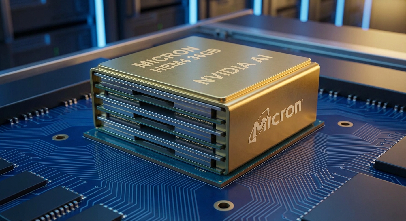
Micron has begun high-volume shipments of HBM4 36GB 12-high memory modules, a core component of NVIDIA's Vera Rubin platform. The HBM4 modules deliver speeds exceeding 11 Gb/s with bandwidth of over 2.8 TB/s — a 2.3x performance increase over HBM3E while consuming 20% less power. The achievement represents a major milestone for Micron, which trailed SK Hynix in HBM3 market share but has closed the gap significantly with its fourth-generation technology. Micron also revealed it has started sampling 48GB 16-high HBM4 stacks for future platforms, pushing the boundaries of through-silicon via (TSV) technology and thermal management in vertically stacked memory.
The AI memory supercycle drove Micron to a massive Q2 2026 earnings beat, with HBM revenue becoming the fastest-growing segment in the company's history. HBM4 revenue alone contributed $2.8 billion in the quarter, a figure that exceeded Micron's entire HBM revenue for all of 2024. CEO Sanjay Mehrotra told analysts that HBM demand visibility now extends through 2028, with every major AI accelerator platform — including NVIDIA Rubin, AMD MI400, and Google TPU v6 — requiring increasing amounts of high-bandwidth memory per chip. Micron's gross margins on HBM4 are estimated at 55-60%, significantly higher than its traditional DRAM business, making HBM the most profitable product category in the company's portfolio.
SK Hynix is evaluating ASML's High-NA EUV technology for future HBM4 production to achieve tighter patterning and higher stacking density. The competition between Micron and SK Hynix for NVIDIA's HBM allocation has intensified, with Samsung also fighting to qualify its own HBM4 modules after struggling with HBM3E yields. Industry analysts project the total HBM market will reach $45 billion by 2027, up from just $4 billion in 2023, representing the most dramatic market expansion in memory industry history. The strategic importance of HBM has elevated memory companies from commodity suppliers to essential partners in the AI ecosystem, fundamentally changing the power dynamics in the semiconductor value chain.
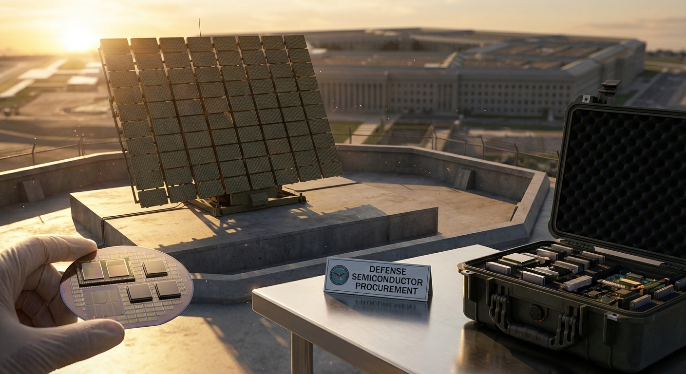
The U.S. Department of Defense has activated emergency procurement protocols for radiation-hardened and military-grade semiconductors, with defense chip orders surging 60% year-over-year since the Iran conflict intensified. The Pentagon's primary concern centers on precision-guided munitions, which require specialized FPGAs and ASICs manufactured on trusted foundry processes, and electronic warfare systems that depend on gallium nitride (GaN) and silicon carbide (SiC) chips. Northrop Grumman, Raytheon, and Lockheed Martin have all placed expedited orders with defense-qualified foundries including GlobalFoundries' Fab 9 in Vermont and Intel's secure enclave at Fab 52. The Trusted Foundry program, which ensures chips for classified systems are manufactured domestically, is now operating at maximum capacity for the first time since its establishment.
Israel's defense sector has simultaneously placed record semiconductor orders, driving a 40% increase in demand at Tower Semiconductor's Migdal HaEmek fab. Iron Dome missile defense interceptors alone consume an estimated 200-300 custom ASICs per unit, and production rates have tripled since hostilities began. The U.S. has also expedited shipments of Patriot missile batteries and THAAD systems to regional allies, each requiring hundreds of specialized radar processing chips, signal processors, and hardened communications ICs. Defense primes are reportedly paying 3-5x commercial spot prices to secure priority allocation at foundries, further squeezing availability for commercial customers already facing tight supply conditions.
The conflict has reignited Congressional debate over the CHIPS Act's defense provisions and whether the U.S. needs a dedicated military semiconductor fabrication facility. A bipartisan group of senators has introduced the SHIELD Chips Act, which would allocate $4.5 billion specifically for defense-grade semiconductor manufacturing capacity, separate from the commercial CHIPS Act funding. GlobalFoundries CEO Thomas Caulfield testified before the Senate Armed Services Committee that current domestic capacity for radiation-hardened chips meets only 65% of projected wartime demand, creating a dangerous gap that adversaries could exploit. The Pentagon's Defense Innovation Unit (DIU) has also fast-tracked contracts with three startups developing novel chiplet-based approaches to defense semiconductors that could reduce lead times from 18 months to under 6 months.
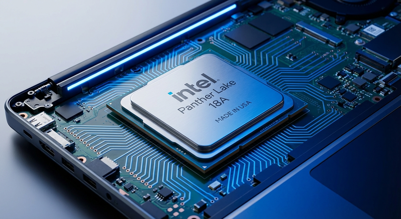
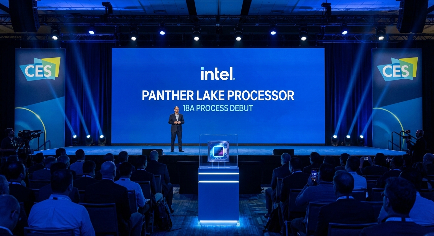
Intel has begun shipping its Panther Lake processors to retail partners worldwide, marking the first commercial arrival of the Intel 18A process node — the most advanced semiconductor ever manufactured in the United States. Debuted at CES 2026, Panther Lake delivers 50% faster CPU performance and 50% faster graphics over the previous generation, with 180 TOPS total platform AI performance. Over 200 laptop designs are in development across Intel's OEM partners including Dell, HP, Lenovo, and Asus, with initial models targeting the premium ultrabook and mobile workstation segments where Intel's AI capabilities can command price premiums.
However, 18A yields remain below profitable levels and are not expected to reach cost thresholds until late 2026. Industry sources estimate current yields at approximately 40-50%, compared to the 70%+ typically needed for volume profitability. This means Intel is effectively subsidizing each Panther Lake chip sold in the near term, a calculated investment to demonstrate 18A's viability to both OEM partners and potential external foundry customers. CEO Lip-Bu Tan has called 2026 an execution year, with Intel's growth inflection point targeted for 2027. Early benchmark results have been encouraging, with Panther Lake outperforming AMD's Ryzen 9000 series in several key workloads and matching Apple's M4 Pro in single-threaded performance.
The company is reconsidering offering 18A to external foundry customers alongside the upcoming 14A node, a decision that could fundamentally reshape Intel's business model. The success or failure of Panther Lake in the market will be closely watched as a leading indicator of Intel's broader turnaround strategy. Wall Street analysts remain divided: bulls argue that 18A represents a genuine technological achievement that will attract foundry customers, while bears point to the yield challenges and note that Intel has a history of promising process node breakthroughs that arrive late or underperform. Intel's stock has traded in a wide $18-32 range over the past six months, reflecting this fundamental uncertainty about the company's trajectory.
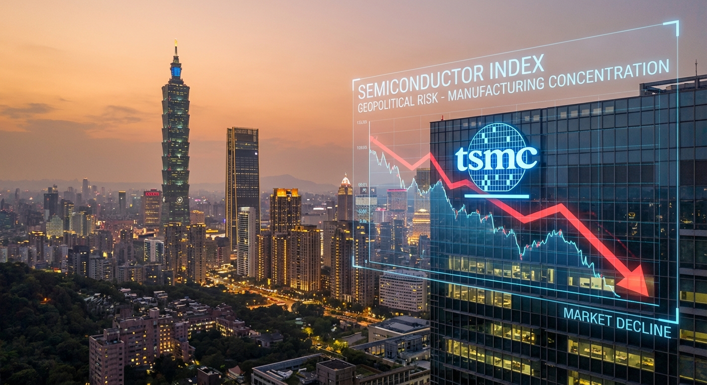
The Iran conflict has reignited investor anxiety over the semiconductor industry's overwhelming dependence on Taiwan, with TSMC shares falling 8% in a single week as fund managers reassess geopolitical concentration risk. The logic is straightforward: if a regional conflict in the Persian Gulf can disrupt global supply chains this severely, what would happen if tensions escalated in the Taiwan Strait? TSMC manufactures over 90% of the world's most advanced chips below 7nm, and any disruption to its operations would be catastrophic for the global economy. Morgan Stanley estimates that a six-month interruption to TSMC's output would cause $1.5 trillion in economic damage worldwide.
The fear premium has accelerated capital flows into "de-risking" plays: Intel and Samsung foundry stocks have rallied 12% and 9% respectively, while the U.S., Japan, and EU have all announced expedited timelines for domestic fab construction. TSMC's own geographic diversification — with fabs under construction in Arizona, Japan, and Germany — has taken on renewed urgency, though none of these facilities will reach leading-edge production before 2028. Hedge fund managers are increasingly building "Taiwan tail risk" positions, purchasing out-of-the-money put options on TSMC ADRs and semiconductor ETFs as insurance against a worst-case scenario. BlackRock's semiconductor portfolio strategy team has reportedly shifted $8.5 billion in allocation toward geographically diversified chipmakers, favoring companies with multi-region manufacturing footprints.
The broader geopolitical calculus is sobering. China conducted naval exercises in the Taiwan Strait within days of the Iran conflict's escalation, a move analysts interpreted as a signal that Beijing is closely monitoring how the West responds to simultaneous geopolitical pressures. Taiwan's Ministry of Economic Affairs has responded by accelerating a "silicon shield" contingency plan that would ensure critical TSMC intellectual property and key personnel could be relocated in an emergency scenario. Meanwhile, the White House has quietly assembled a task force to model the economic impact of various Taiwan contingency scenarios, with preliminary findings suggesting that even a 90-day disruption to TSMC's leading-edge output would trigger a global recession comparable to 2008. The Iran conflict has transformed what was previously an abstract geopolitical risk into a viscerally real concern for semiconductor investors worldwide.
Intel has reversed course and is now offering its 18A process node to external foundry customers — a significant pivot after CEO Lip-Bu Tan had previously reserved it for internal use only. CFO David Zinsner said yield improvements of 7–8% per month are now materializing, making 18A viable for outside clients, while the more advanced 14A node will only receive investment once major external customers are secured. Intel's foundry business is targeting break-even operating margins by end of 2027.
ASML's High-NA EUV lithography system, the EXE:5200B, is now in active deployment across the semiconductor industry. Intel has taken the lead, using the machine to pattern its upcoming 14A process node, positioning the company at the forefront of EUV lithography adoption. The High-NA system features a 0.55 numerical aperture (up from 0.33 on standard EUV), enabling finer patterning resolution of 8nm half-pitch — a capability essential for manufacturing transistors at the 2nm node and below. Samsung is receiving its first High-NA EUV system in early 2026, with plans to integrate it into advanced foundry production lines at its Pyeongtaek campus.
Meanwhile, SK Hynix is evaluating the technology for future HBM4 memory production, where tighter patterning could enable higher stacking density and faster interconnects. Each EXE:5200B system costs upward of $380 million, weighs over 150 metric tons, and requires a dedicated building wing for installation — making ASML the most critical equipment supplier in the entire chip manufacturing ecosystem. ASML's order backlog now exceeds $40 billion, with delivery slots booked through 2028, giving the Dutch company unprecedented visibility into the semiconductor industry's capital expenditure trajectory. TSMC has ordered at least 20 High-NA systems for its upcoming A14 and A16 process nodes, representing over $7.6 billion in equipment spending from a single customer.
The High-NA EUV rollout has significant implications for the competitive landscape. Intel's early adoption gives it a potential process technology advantage in patterning capability, even if its overall manufacturing ecosystem lags TSMC's. ASML CEO Christophe Fouquet has stated that the company is already developing the next-generation Hyper-NA system with a 0.75 numerical aperture, targeted for deployment around 2030. The concentration of cutting-edge lithography capability in a single company — ASML holds a 100% monopoly on EUV systems — represents both a strategic vulnerability and a powerful chokepoint in global semiconductor supply chains. Geopolitical pressure on the Netherlands to restrict ASML sales to China has intensified, with the Dutch government now requiring export licenses for both High-NA and standard EUV systems destined for Chinese customers.
At GTC 2026, CEO Jensen Huang unveiled that Vera Rubin — NVIDIA's next-generation AI platform built on TSMC's 3nm process with 336 billion transistors — is now in full production and will reach cloud partners in the second half of 2026. Huang projected combined purchase orders for Blackwell and Vera Rubin will hit $1 trillion through 2027. Looking ahead, Rubin Ultra (2027) will double performance to 100 petaflops with 500 billion transistors and the new Kyber rack design, while the Feynman architecture rounds out NVIDIA's roadmap to 2028.
The U.S. Treasury Department and European Council have jointly announced expanded sanctions targeting Iran's access to semiconductor technology, AI accelerators, and advanced computing equipment. The new measures prohibit the sale or transfer of any semiconductor manufacturing equipment, EDA software tools, and chips above 100 TOPS of AI compute performance to Iranian entities. ASML, Applied Materials, Lam Research, and KLA Corporation are all directly affected by the export controls. The sanctions also target third-party intermediaries in the UAE, Turkey, and Central Asia that have facilitated technology transfers to Iran. Synopsys and Cadence have been directed to revoke any active EDA licenses held by Iranian universities or research institutions.
The tech sanctions are modeled on the China chip export control framework but applied more broadly, covering not just leading-edge technology but also mature-node equipment down to 28nm. This is a significant escalation from previous Iran sanctions, which primarily focused on financial instruments and energy exports. The Bureau of Industry and Security (BIS) has added 47 Iranian entities to the Entity List, including the Iranian Electronics Industries (IEI), several university research labs, and military-affiliated technology procurement organizations. U.S. officials have cited intelligence indicating that Iran was using imported semiconductor equipment to produce guidance system components and drone navigation chips, leveraging technology originally acquired through third-party shell companies in Dubai and Istanbul.
Industry analysts note that while Iran is not a significant semiconductor market — estimated at under $800 million annually — the sanctions signal a broader trend of technology becoming a primary instrument of geopolitical pressure alongside traditional economic and military measures. The practical enforcement challenge is substantial: the semiconductor supply chain involves thousands of intermediaries, and Iran has demonstrated sophistication in circumventing technology export controls through front companies and transshipment hubs. The Semiconductor Industry Association (SIA) has expressed cautious support for the sanctions while warning that overly broad restrictions could create compliance burdens for U.S. chipmakers that far exceed the strategic benefit, particularly if the controls inadvertently disrupt legitimate trade with allied nations in the region.
Samsung Foundry is in discussions with Intel to form a strategic partnership centered on advanced packaging technologies and glass substrate development, according to multiple industry sources. The alliance aims to create a viable alternative to TSMC's dominant CoWoS advanced packaging platform, which currently commands over 50% of the global capacity for high-bandwidth AI accelerator packaging. Samsung and Intel are exploring joint development of next-generation glass substrates that could offer superior electrical performance and thermal characteristics compared to traditional organic substrates, with initial prototypes reportedly achieving 2x the wiring density and 50% better signal integrity at high frequencies.
If formalized, the partnership would represent a historic alignment between two of TSMC's largest competitors, combining Samsung's memory expertise and foundry scale with Intel's advanced packaging research and its EMIB and Foveros technologies. The complementary nature of the two companies' capabilities is compelling: Samsung leads in HBM memory stacking, while Intel has pioneered die-to-die interconnect technologies that are critical for chiplet-based architectures. Together, they could offer a complete alternative packaging ecosystem for AI accelerators that currently have no choice but to use TSMC's CoWoS platform.
Industry analysts have cautioned that any Samsung-Intel packaging alliance would face significant execution challenges, including the need to harmonize different manufacturing standards, IP sharing concerns, and the 3-5 year timeline typically required to qualify new packaging platforms with major customers. However, the strategic imperative is clear: NVIDIA, AMD, and hyperscaler custom chip teams are all actively seeking second-source packaging options to reduce their dependence on TSMC. If Samsung and Intel can deliver a competitive alternative, they could unlock a combined $15-20 billion annual market opportunity in advanced packaging services that is currently almost entirely captured by TSMC. The discussions reportedly accelerated after TSMC imposed allocation limits on CoWoS capacity that forced several major customers to delay product launches.
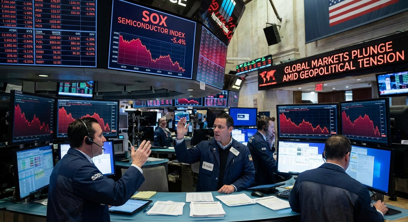
The Philadelphia Semiconductor Index (SOX) recorded its worst weekly performance since October 2022, shedding 11.4% as investors priced in the cascading effects of the Iran conflict on the global chip industry. NVIDIA led the decline, falling 14% on concerns that shipping disruptions could delay Vera Rubin platform deliveries. ASML dropped 12% despite its record backlog, as analysts flagged potential delays in High-NA EUV system installations due to component supply issues. AMD fell 10%, Qualcomm shed 9%, and Broadcom declined 8%. The only bright spots were defense-exposed chipmakers: Microchip Technology and Texas Instruments, both major suppliers of military-grade components, rallied 6% and 4% respectively.
Hedge funds have increased short positions on the semiconductor sector by $18 billion in the past two weeks, the largest bearish bet since the 2022 downturn. Options market data shows implied volatility on the SOX index surging to 45%, levels not seen outside of the COVID crash and the 2022 rate-hike cycle. The VanEck Semiconductor ETF (SMH) experienced its largest single-day outflow on record at $2.3 billion, as retail and institutional investors alike rushed to reduce exposure. Put-to-call ratios on NVIDIA and AMD options reached 2.1x and 1.8x respectively, indicating deeply bearish sentiment across the sector.
However, contrarian analysts argue the selloff is overdone — JPMorgan maintained an "overweight" rating on the semiconductor sector, noting that the structural demand drivers from AI remain intact and that any supply disruption would ultimately lead to higher pricing power for chipmakers. Goldman Sachs issued a note titled "Buy the Fear" arguing that geopolitical selloffs in semiconductors have historically reversed within 60-90 days, with the sector outperforming its pre-shock levels by an average of 18% within six months. Berkshire Hathaway's latest 13F filing revealed that Warren Buffett's firm added to its TSMC position during the dip, a move interpreted as a strong contrarian signal by market watchers. The fundamental tension remains between short-term supply chain disruption risk and the long-term reality that global semiconductor demand is on a structural growth trajectory driven by AI, electrification, and digital transformation.
The race for next-generation high-bandwidth memory has entered production. SK Hynix has commenced mass production of HBM4, the fourth generation of its high-bandwidth memory technology, which offers substantially higher data transfer speeds and capacity per stack compared to HBM3E. The HBM4 specification supports up to 2 TB/s of bandwidth per stack with a 2048-bit wide interface, roughly double the bandwidth of HBM3E, while simultaneously improving power efficiency by 30% through lower operating voltages and advanced power management circuits. SK Hynix's initial HBM4 products feature 12-high stacks delivering 36 GB per module, with 16-high 48 GB variants expected by Q4 2026.
Samsung, not to be outdone, showcased its own HBM4 technology at NVIDIA's GTC 2026 conference, demonstrating working samples and announcing partnerships with multiple chip manufacturers. Samsung's approach differentiates itself through a hybrid bonding interconnect that eliminates traditional micro-bumps between memory layers, enabling tighter stacking pitches and theoretically higher bandwidth density. However, industry sources indicate Samsung's HBM4 yields are currently 15-20 percentage points below SK Hynix's, and full NVIDIA qualification is not expected until Q3 2026 at the earliest. The qualification gap has allowed SK Hynix to maintain its dominant 50%+ share of the HBM market, with Micron holding approximately 30% and Samsung trailing at 20%.
The HBM4 generation is critical for enabling the next wave of large language model training, where memory bandwidth has become as important as raw compute performance. Models with over 2 trillion parameters require massive memory capacity and bandwidth to efficiently distribute training data across GPU clusters, and HBM4's specifications are specifically designed to eliminate the memory wall that has constrained AI training throughput. Both companies are investing billions in expanding their advanced packaging capabilities to stack more memory layers — SK Hynix alone is spending $11 billion on a new HBM-focused fab in Icheon, South Korea, scheduled to begin production in 2027. The total addressable market for HBM is projected to grow from $16 billion in 2025 to over $45 billion by 2028, making it the highest-growth segment in the entire memory industry.
The Iran conflict is hitting the AI industry through two vectors simultaneously: surging energy costs for power-hungry data centers and delayed deliveries of GPU servers and networking equipment. Microsoft, Google, Amazon, and Meta — which collectively planned $280 billion in AI infrastructure spending for 2026 — are now reassessing their capital expenditure timelines. Data center electricity costs have risen 20-25% in regions dependent on fossil fuel generation, with some hyperscalers reportedly activating diesel backup generators to maintain operations during grid instability events in Asia. The GPU shortage, already severe before the conflict, has worsened as shipping delays push back NVIDIA Blackwell and upcoming Rubin deliveries by 4-6 weeks.
OpenAI CEO Sam Altman told investors that training costs for GPT-5.5 could increase by $200-400 million if the energy situation persists. Anthropic and Google DeepMind have both delayed planned training runs for next-generation models. Microsoft Azure has reportedly paused expansion of two planned data center campuses in Southeast Asia due to uncertain power costs, while Amazon Web Services is accelerating construction of nuclear-powered data center facilities in the eastern United States as a hedge against fossil fuel volatility. Meta's infrastructure team has begun exploring on-site small modular reactor (SMR) deployments for its largest AI training clusters, a strategy that would take years to implement but reflects the severity of the energy cost concern.
The downstream effects on AI development timelines are already visible. Several major AI labs have shifted compute allocation from training new models to optimizing inference efficiency on existing ones, a pragmatic response to the higher per-hour cost of GPU cluster operation. Analysts at Morgan Stanley estimate that the total incremental cost to the AI industry from the Iran conflict could reach $35-50 billion in 2026, encompassing higher energy bills, delayed hardware deliveries, and increased component costs. The conflict underscores the fragility of the AI boom's dependence on a complex, globally distributed hardware supply chain that runs from oil wells in the Persian Gulf to chip fabs in Taiwan to data centers in Virginia. It also strengthens the argument for energy-independent AI infrastructure, a trend that was already emerging but has now become a boardroom priority at every major technology company.
Samsung Foundry has secured one of the largest chip manufacturing contracts in semiconductor history: an eight-year, $16.5 billion deal to produce Tesla's AI6 automotive chips. Elon Musk disclosed the arrangement while also revealing that Tesla's current AI5 generation chips are manufactured through a split allocation between Samsung Foundry and TSMC. The AI6 contract represents a major validation for Samsung's advanced process nodes and its ability to serve the automotive semiconductor market at scale, a segment that requires uniquely stringent reliability standards including AEC-Q100 qualification and zero-defect quality targets.
The deal is expected to utilize Samsung's Taylor, Texas fabrication facility once it reaches full operational status, aligning with U.S. government incentives under the CHIPS Act to onshore critical chip manufacturing capacity. Tesla's AI6 chip is designed to power Level 5 fully autonomous driving, requiring over 500 TOPS of neural network inference performance while operating within the strict thermal and power constraints of an automotive environment. The chip will integrate custom AI accelerator cores designed by Tesla's in-house silicon team alongside Arm-based CPU clusters and a dedicated vision processing unit capable of fusing data from 12 cameras, 6 radars, and 3 LiDAR sensors simultaneously.
For Samsung, the Tesla win partially offsets the loss of key mobile SoC clients to TSMC in recent years and demonstrates that the company can compete for the highest-value foundry contracts in the industry. Analysts at Bernstein estimate that the deal will contribute approximately $2 billion annually to Samsung Foundry's revenue starting in 2028, representing a meaningful step toward the division's goal of achieving profitability by 2029. The automotive semiconductor market is projected to reach $120 billion by 2030, and Samsung's Tesla partnership positions it as a credible player in a segment that has historically been dominated by specialized IDMs like NXP, Infineon, and Texas Instruments rather than pure-play foundries.
TSMC reported January–February revenue growth of 30% year-over-year, driven by surging AI chip demand from NVIDIA, Apple, and AMD. The company's HPC segment — which captures AI data center orders — grew 48% and now represents 58% of total revenue. TSMC's 2nm node is entering mass production in the second half of 2026 and is expected to outpace 3nm adoption from the start, while SoIC advanced packaging capacity is being expanded to 10,000–15,000 wafers per month to support next-generation AI accelerators.
The Iran conflict has transformed the political calculus around domestic semiconductor manufacturing, with the administration announcing an emergency acceleration of $8 billion in additional CHIPS Act disbursements to fast-track U.S. fab construction. Commerce Secretary Howard Lutnick stated that the conflict "validates everything we warned about regarding the fragility of global chip supply chains" and announced streamlined permitting processes for fab construction in Arizona, Ohio, New York, and Texas. Intel's Fab 52 and Fab 62 in Arizona, TSMC's Phoenix facility, and Samsung's Taylor fab have all been designated as "critical national security infrastructure," qualifying them for expedited environmental reviews and accelerated construction timelines.
Japan has followed suit, announcing an additional $5 billion for Rapidus and TSMC's Kumamoto operations, while South Korea has pledged $3.2 billion in emergency subsidies to Samsung and SK Hynix to ensure uninterrupted domestic production. The European Chips Act is also being amended to increase total funding by 30%, with Germany's Saxony region and France's Grenoble cluster identified as priority sites for expanded capacity. India has accelerated its semiconductor incentive program, fast-tracking approvals for the Tata-PSMC fab in Gujarat and offering additional tax breaks to attract TSMC or Samsung to establish a presence on the subcontinent. The global race for semiconductor sovereignty has never been more intense.
The geopolitical shock has created bipartisan consensus that semiconductor self-sufficiency is no longer a long-term aspiration but an immediate national security imperative. A rare joint statement from the Senate Commerce and Armed Services committees called for doubling the original CHIPS Act funding over the next five years, bringing total U.S. semiconductor investment support to over $100 billion. Construction timelines that were previously measured in 4-5 year horizons are being compressed to 2.5-3 years through emergency permitting, 24/7 construction shifts, and modular fab building techniques pioneered by TSMC in Taiwan. The workforce challenge remains acute, however, with an estimated shortage of 67,000 skilled semiconductor workers in the United States alone — a gap that no amount of funding can close overnight and that represents the single biggest bottleneck to the reshoring ambition.
Samsung Foundry has begun running sample silicon tests with AMD on its second-generation 2nm process node, known as SF2P, which incorporates performance optimizations over the baseline SF2 technology. The SF2P process reportedly delivers an additional 5-8% performance improvement at the same power envelope, achieved through refined channel strain engineering and optimized nanosheet dimensions. The collaboration signals AMD's willingness to diversify its chip manufacturing beyond TSMC, potentially for specific product lines where capacity access matters more than cutting-edge density — a pragmatic approach given the severe allocation constraints at TSMC's most advanced nodes.
Separately, Google's TPU hardware team reportedly visited Samsung's Taylor, Texas fabrication facility to evaluate the company's readiness for producing custom AI accelerators. The Google visit is particularly notable given that TSMC's CoWoS capacity constraints have forced Google to scale back its TPU v6 production targets by an estimated 30%. Sources indicate that Google engineers spent three days at the Taylor facility, evaluating Samsung's 2nm process capabilities, advanced packaging options, and quality control systems. Samsung demonstrated its I-Cube4 packaging technology, which can integrate up to four logic dies with eight HBM stacks on a single interposer — a configuration well-suited to Google's TPU architecture.
Samsung is positioning itself as a viable second source for hyperscaler AI silicon, leveraging its integrated memory and logic capabilities as a key differentiator that neither TSMC nor Intel can match. The ability to co-optimize HBM memory and logic die manufacturing within the same company could yield performance and cost advantages for customers willing to source both from Samsung. Industry analysts estimate that if Samsung secures even one major hyperscaler AI chip contract, it could add $4-6 billion in annual foundry revenue and fundamentally alter the competitive dynamics of the advanced foundry market, where TSMC currently commands an overwhelming 90%+ share of chips below 7nm.
Intel Foundry Services has confirmed that it now has four external customers committed to using its manufacturing capabilities, a meaningful milestone for a business unit that only began courting outside clients in earnest three years ago. The Intel 18A process node is being used internally for both Panther Lake consumer processors and Clearwater Forest server chips, with production running at Fab 52 in Chandler, Arizona. While Intel has not disclosed the identities of all external customers, the IBM win and ongoing discussions with NVIDIA suggest the company is making progress in its ambition to become a top-three foundry by 2030.
Sources familiar with Intel's foundry pipeline indicate that in addition to IBM, the four external customers include at least one major U.S. defense contractor and one European automotive chipmaker, both drawn to Intel's U.S.-based manufacturing for supply chain security reasons. The fourth customer is believed to be a mid-sized fabless AI chip startup that valued Intel's willingness to offer lower minimum order quantities than TSMC, which typically requires commitments of 10,000+ wafers per quarter for leading-edge nodes. Intel Foundry's revenue from external customers is expected to reach $1 billion in 2026, a modest figure compared to TSMC's $80+ billion but a significant proof point for the viability of Intel's foundry strategy.
The foundry market remains overwhelmingly dominated by TSMC, which commands roughly 60% market share, but Intel's combination of U.S.-based manufacturing and competitive process technology is attracting interest from customers concerned about geographic concentration of chip manufacturing in East Asia. Intel CEO Lip-Bu Tan has set a target of $10 billion in external foundry revenue by 2030, which would require winning at least 2-3 additional marquee customers in the next 18 months. The company's pitch centers on three pillars: the technical competitiveness of 18A and upcoming 14A nodes, the geopolitical advantage of domestic U.S. manufacturing, and generous capacity guarantees that TSMC's oversubscribed fabs cannot match. Whether Intel can execute on this ambitious plan while simultaneously fixing its own product competitiveness issues remains the central question for the company's future.
Samsung's massive fabrication facility expansion in Taylor, Texas has reached 93.6% physical completion, with the company now targeting July 2026 for the start of chip manufacturing operations. The total investment has ballooned to $44 billion, making it one of the single largest semiconductor manufacturing investments ever undertaken on U.S. soil. Samsung has secured $6.6 billion in direct funding under the U.S. CHIPS and Science Act, which mandates domestic production of advanced chips. The Taylor fab spans over 5 million square feet and will employ approximately 4,500 workers at full operation, with another 6,000 indirect jobs created in the surrounding community.
The Taylor fab is expected to produce chips on Samsung's 4nm and 2nm process nodes, serving automotive, AI, and high-performance computing customers. The facility features Class 1 cleanrooms with the most advanced contamination control systems available, designed to support gate-all-around nanosheet transistor manufacturing from day one. ASML has delivered multiple EUV lithography systems to the site, with High-NA EUV tools scheduled for installation in 2027 to enable sub-2nm production. Samsung has also built a dedicated advanced packaging facility adjacent to the main fab, capable of performing wafer-level chip stacking and 2.5D interposer integration — capabilities that are increasingly essential for AI accelerator production.
The project has faced multiple delays since its original 2024 target date, but Samsung management has stated that the current timeline is firm and equipment installation is now in its final phase. Local officials in Williamson County have noted that the Samsung investment has triggered a broader semiconductor ecosystem buildout, with over 40 supplier companies establishing operations within a 50-mile radius of the Taylor facility. The Texas state government has provided an additional $1.2 billion in property tax abatements and infrastructure support, making the total public incentive package for Samsung's Taylor operations one of the most generous in U.S. industrial history. The fab's success will be a critical test of whether Samsung can compete with TSMC on American soil.
The overwhelming demand for TSMC's advanced nodes and CoWoS advanced packaging has created a capacity crunch that is forcing even the foundry's largest customers to explore alternatives. NVIDIA and Broadcom, two of the biggest consumers of TSMC silicon, are both actively evaluating Intel Foundry and Samsung Foundry for portions of their future chip manufacturing needs. TSMC's advanced node utilization rates are running at over 100% when accounting for wafer starts versus nameplate capacity, and the company has told customers that meaningful additional 3nm and 2nm capacity will not be available until mid-2027 at the earliest.
The situation echoes the chip shortage of 2021-2022 but is concentrated at the leading edge rather than across the entire semiconductor supply chain. TSMC's allocation committee — an internal body that determines which customers receive wafer starts — has become one of the most powerful decision-making groups in the technology industry, with the ability to accelerate or delay billions of dollars in product launches from the world's largest chipmakers. Companies that historically had guaranteed allocations are now finding themselves rationed, creating frustration and urgency to secure alternative manufacturing sources.
For Intel and Samsung, the TSMC bottleneck represents a strategic opportunity to win business that might otherwise never have been available. Intel Foundry chief Kevin O'Buckley has reportedly held over 40 meetings with TSMC customers in the past quarter alone, offering aggressive pricing, guaranteed capacity commitments, and the geopolitical advantage of U.S.-based manufacturing. Samsung is making a similar pitch, emphasizing its integrated memory-logic capabilities and competitive 2nm GAA technology. Industry analysts note that even capturing 5-10% of overflow demand from TSMC's top customers would represent billions in revenue for either competitor and could reshape the competitive dynamics of the foundry market for years to come. The fundamental question is whether customers currently forced to explore alternatives will return to TSMC once capacity expands, or whether this moment represents a genuine and lasting shift toward a more balanced foundry ecosystem.
TSMC's CoWoS (Chip-on-Wafer-on-Substrate) advanced packaging platform has become the single most contested resource in the semiconductor supply chain. NVIDIA has secured commitments for more than 50% of TSMC's total CoWoS capacity through 2027, reflecting the staggering demand for its H200, B200, and upcoming Rubin-series data center GPUs. The lock-up is valued at an estimated $12-15 billion in packaging services revenue alone, separate from the silicon wafer processing fees. TSMC's CoWoS capacity has expanded from 15,000 wafer equivalents per month in early 2025 to approximately 40,000 wafer equivalents per month currently, yet demand still exceeds supply by an estimated 30%.
The lock-up has created a ripple effect across the industry: Google has reportedly been forced to reduce its TPU production targets due to insufficient CoWoS allocation, while other hyperscalers including Amazon and Microsoft are competing for the remaining slots. AMD's MI400 ramp has also been constrained by packaging availability rather than wafer supply, a frustrating bottleneck for a company that finally has a competitive AI accelerator product. Broadcom, which designs custom AI chips for Google and other hyperscalers, has had to delay at least two major customer programs due to CoWoS allocation limitations.
TSMC is aggressively expanding CoWoS capacity with three new advanced packaging facilities under construction in Taiwan, but the technology requires specialized equipment and cleanroom space that cannot be deployed overnight. The advanced packaging bottleneck has become a more significant constraint than the silicon wafer supply itself for AI accelerator production — a paradigm shift that has caught many industry observers off guard. TSMC's advanced packaging revenue is projected to reach $15 billion in 2026, up from $4 billion in 2023, making it one of the fastest-growing segments in the entire semiconductor industry. The packaging bottleneck has also opened a strategic window for competitors: Samsung's I-Cube and Intel's EMIB/Foveros technologies are being evaluated by customers who cannot secure sufficient TSMC CoWoS allocation, potentially breaking TSMC's near-monopoly in advanced AI chip packaging.
The global foundry market is projected to reach $202 billion in 2026, with forecasts showing continued expansion to $263.1 billion by 2034, according to industry research from TrendForce and IC Insights. The growth trajectory is being propelled by insatiable demand for AI training and inference chips, automotive semiconductors, and the ongoing transition to advanced process nodes below 5nm. AI-related foundry revenue alone is expected to account for $62 billion in 2026, up from just $18 billion in 2023 — a compound annual growth rate of over 50% that dwarfs every other semiconductor end-market category.
TSMC continues to command the lion's share of foundry revenue at approximately 60% market share, with Samsung holding roughly 13%, GlobalFoundries at 6%, and Intel Foundry growing from a negligible base. The market structure increasingly favors companies that can offer both leading-edge silicon wafer processing and advanced packaging solutions, as the performance of modern chips depends as much on how they are assembled as on the transistors themselves. TSMC's dominance is most extreme at the leading edge, where it captures over 90% of all sub-7nm revenue, but competition is more balanced at mature nodes where GlobalFoundries, UMC, and SMIC all maintain significant positions.
Geographic diversification is also reshaping the market, with new fabs under construction in the United States, Japan, and Europe. The total global investment in new semiconductor manufacturing capacity between 2024 and 2030 is projected to exceed $1 trillion, driven by a combination of private capital expenditure and government subsidies. Mordor Intelligence estimates that the foundry market's growth rate will remain above 8% CAGR through 2034, sustained by the proliferation of AI into every sector of the economy, the electrification of transportation, the expansion of cloud computing, and the emerging demand for chips in space and satellite applications. The foundry market has evolved from a niche manufacturing service into the backbone of the global technology economy, and the companies that control advanced chip manufacturing capacity now wield influence comparable to the oil majors of the 20th century.
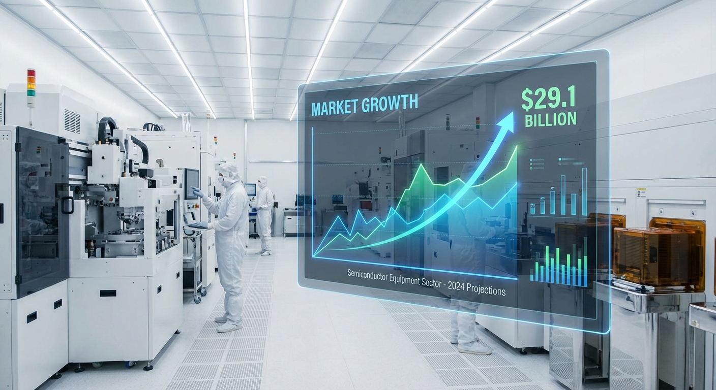
The global semiconductor equipment market has reached $29.1 billion in 2026, growing at a compound annual growth rate of 10.1% and projected to hit $42.76 billion by 2030, according to new industry analysis. The growth is being driven by massive capital expenditure from TSMC, Samsung, and Intel as they race to build out capacity for advanced process nodes and advanced packaging technologies. TSMC alone has committed to $38-40 billion in capex for 2026, the largest single-year investment by any semiconductor company in history, with approximately 70% allocated to leading-edge 2nm and 3nm capacity and the remainder split between advanced packaging expansion and specialty technology nodes.
EUV lithography equipment from ASML accounts for a disproportionate share of the spending, with each High-NA system priced above $380 million and standard EUV systems at $200 million each. Beyond lithography, the transition to gate-all-around nanosheet transistors has created surging demand for atomic layer deposition (ALD) and atomic layer etch (ALE) tools from Applied Materials and Lam Research, as GAA architectures require atomic-precision material deposition around complex 3D channel structures. KLA Corporation's inspection and metrology tools have also seen record demand, as the shrinking margin for manufacturing defects at 2nm makes quality control more critical than ever.
Semiconductor stocks have outperformed the broader technology sector year-to-date, with ASML, Applied Materials, and Lam Research all reaching or nearing all-time highs. The equipment sector has become a leading indicator for the broader semiconductor cycle, and the current order trajectory suggests sustained growth through at least 2028. SEMI's World Fab Forecast database now tracks over 90 new fab construction projects worldwide, the highest number in the organization's tracking history, driven by government subsidies from the U.S. CHIPS Act, European Chips Act, Japan's semiconductor strategy, and similar programs in South Korea, India, and Southeast Asia. The equipment supply chain itself is becoming a bottleneck, with lead times for critical tools stretching to 18-24 months and forcing chipmakers to place orders years in advance of planned fab openings.
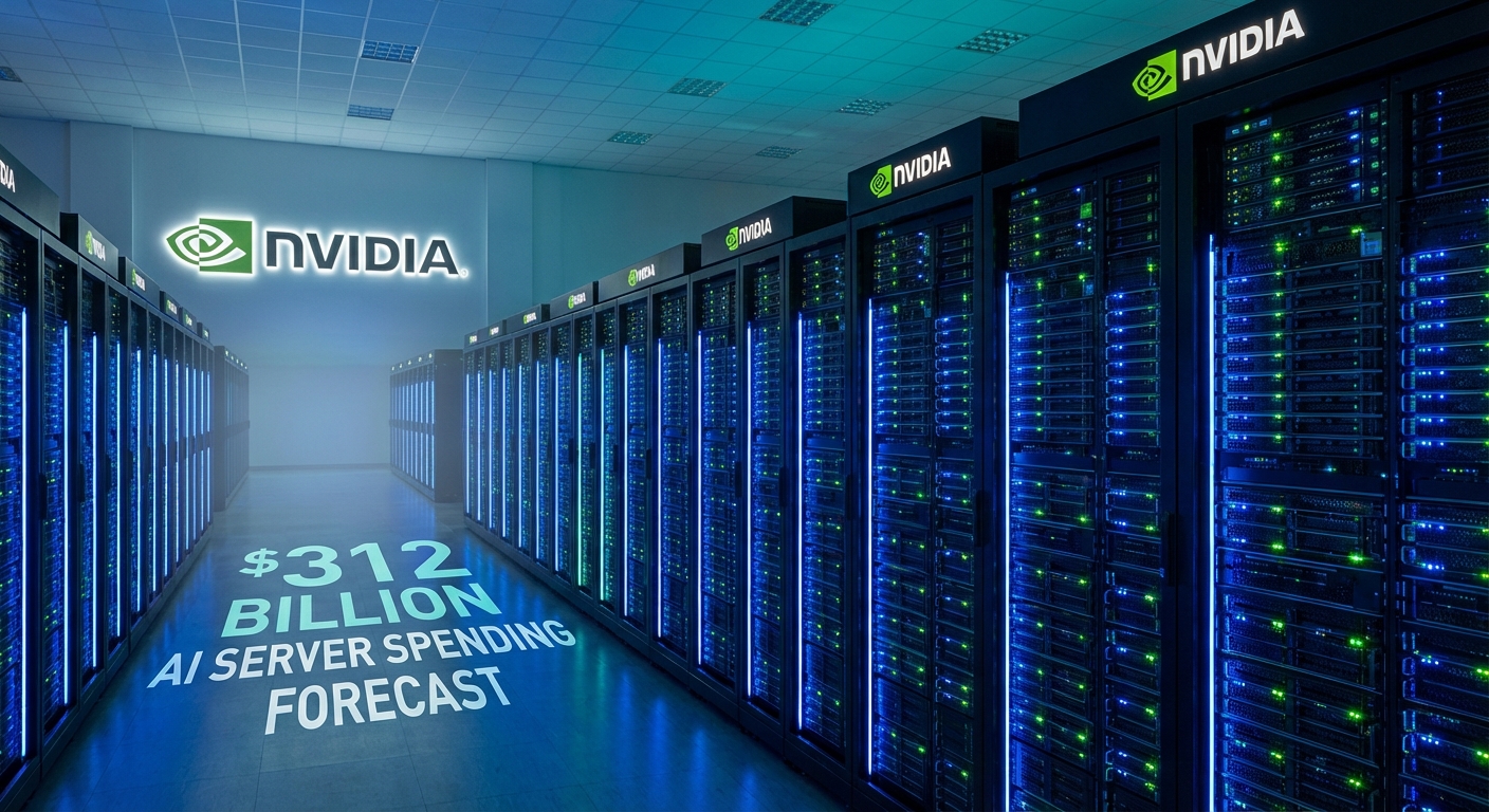
Global spending on AI servers is projected to surge 45% in 2026 to reach $312 billion, according to Bloomberg Intelligence, driven by hyperscaler capital expenditure programs from Microsoft, Google, Amazon, and Meta. The four largest hyperscalers have collectively committed to spending over $280 billion on AI infrastructure this year, with Microsoft leading at $80 billion, followed by Google at $75 billion, Amazon at $70 billion, and Meta at $55 billion. NVIDIA continues to dominate this market with a staggering $275 billion backlog of GPU orders, reflecting demand for its Blackwell and upcoming Rubin-series data center accelerators.
The spending surge has direct implications for the semiconductor supply chain: TSMC, which manufactures the vast majority of NVIDIA chips, is running its advanced nodes at maximum utilization, while HBM4 memory from SK Hynix and Samsung faces its own allocation challenges. Beyond the hyperscalers, a new category of "AI infrastructure companies" including CoreWeave, Lambda, and Crusoe Energy is driving incremental GPU demand, collectively ordering an estimated $40 billion in NVIDIA hardware for 2026-2027 delivery. Sovereign wealth funds from the UAE, Saudi Arabia, and Singapore are also building national AI compute capabilities, adding another layer of demand that barely existed two years ago.
AMD is also capturing an increasing share of the AI accelerator market with its Instinct MI400 series, which offers compelling performance-per-dollar for inference workloads and has secured design wins at Microsoft Azure, Oracle Cloud, and several European supercomputing centers. AMD's AI data center revenue is projected to reach $12 billion in 2026, up from $6.1 billion in 2024, though NVIDIA still commands over 80% of the total AI accelerator market. The scale of AI infrastructure investment has made semiconductor manufacturing the most strategically important industrial sector of the decade, with national security implications that extend far beyond traditional defense applications. Barclays Research estimates that AI-related semiconductor demand will account for 35% of total industry revenue by 2028, up from approximately 20% today, fundamentally reshaping the economics and geopolitics of the chip industry.
TSMC's Arizona fabrication facility has achieved a landmark milestone by producing its first 4nm chips on American soil, marking the most advanced semiconductor node ever manufactured in the United States. Apple and AMD have been confirmed as the initial customers for the fab's N4P process output, with Apple expected to use the chips in future iPhone and Mac products while AMD targets its next-generation EPYC server processors. The Arizona fab, located in north Phoenix, employs over 2,200 engineers and technicians, a mix of TSMC veterans relocated from Taiwan and locally hired American workers trained through an intensive 18-month program developed in partnership with Arizona State University.
Yield rates at the Arizona facility are approaching 90%, significantly ahead of the company's internal schedule and narrowing the gap with TSMC's mature Taiwan fabs faster than analysts anticipated. TSMC chairman Mark Liu stated that the Arizona facility's yield performance "exceeded our most optimistic projections" and credited the success to a hybrid management approach that combines Taiwanese process expertise with American engineering talent. The fab is currently running at approximately 20,000 wafers per month, with plans to scale to 50,000 wafers per month by year-end as additional equipment is installed and qualified.
The success has accelerated plans for a 3nm expansion at the same site, with the administration approving $6.6 billion in CHIPS Act funding to support the next phase of construction. A third fab on the Arizona campus, targeting TSMC's 2nm N2 technology, has also been greenlit for construction starting in late 2026, with production expected in 2029. The total TSMC investment in Arizona is projected to exceed $65 billion, making it one of the largest foreign direct investments in U.S. history. The milestone represents a pivotal moment for the U.S. semiconductor reshoring effort, demonstrating that cutting-edge chip manufacturing can be successfully established outside of East Asia — a proposition that many industry skeptics had questioned given the challenges of replicating Taiwan's semiconductor ecosystem in a new geography.
Samsung has publicly demonstrated its 2nm gate-all-around (GAA) transistor technology, claiming a 25% power efficiency advantage over TSMC's competing N2 process node. The company showcased functional test chips at its annual Samsung Foundry Forum, with mass production targeted for Q4 2026 at its Pyeongtaek campus in South Korea. The test chips demonstrated 3.2 GHz clock speeds on Arm Cortex-A730 cores, with power consumption 25% below equivalent test chips on TSMC's N2, though independent verification of these claims is still pending. Samsung's 2nm GAA process uses four-nanosheet stacks with channel widths ranging from 12nm to 45nm, enabling designers to tune performance and power on a per-transistor basis.
Qualcomm and Google have signed on as early customers, with Qualcomm expected to use the node for its next-generation Snapdragon 9 Gen 5 mobile platform and Google evaluating it for custom TPU accelerators. Samsung also announced a major expansion of its Austin, Texas fabrication facility to bring 2nm GAA production capacity to the United States, leveraging CHIPS Act incentives. The Austin expansion, valued at $12 billion, will add 30,000 wafers per month of 2nm capacity by 2028, complementing the Taylor, Texas facility's focus on automotive and AI chips. Samsung's total U.S. semiconductor investment now exceeds $56 billion, making it the second-largest foreign investor in American chip manufacturing after TSMC.
The 2nm GAA architecture replaces traditional FinFET transistors with nanosheet channels that wrap the gate around all four sides of the channel, enabling superior electrostatic control and significantly reduced leakage current at low voltages. This advantage is particularly relevant for mobile and IoT applications where battery life is paramount. If Samsung can deliver on its yield and performance claims, the 2nm GAA process could represent its strongest competitive position against TSMC in over a decade. However, skeptics point to Samsung's history of overpromising on foundry technology — its 3nm GAA node, launched in 2022, suffered persistent yield issues that drove key customer Qualcomm back to TSMC. Samsung's foundry division must demonstrate that its 2nm execution can match its 2nm ambition, and the Tesla and Qualcomm partnerships will serve as the definitive test of that proposition.
IBM has selected Intel Foundry's 18A process node for the production of its next-generation enterprise and mainframe processors, choosing Intel over Samsung foundry in a decision that carries significant symbolic weight for the semiconductor industry. The Intel 18A node features RibbonFET gate-all-around transistors and PowerVia backside power delivery, offering competitive performance metrics against TSMC's N2 technology. The deal is estimated to be worth $1.5-2 billion over three years, covering IBM's Z-series mainframe processors and next-generation Power architecture server chips used in enterprise AI and financial services workloads.
For Intel Foundry, landing IBM as a customer validates the turnaround strategy that has defined the company's recent transformation under CEO Lip-Bu Tan. IBM brings not only revenue but also credibility — the company invented the semiconductor manufacturing techniques that underpin much of modern chip fabrication, and its endorsement of 18A sends a powerful signal to other potential foundry customers. Intel Foundry chief Kevin O'Buckley stated that IBM's rigorous qualification process, which took over 14 months of testing, provided Intel with invaluable feedback that improved 18A yield and reliability for all customers.
The win also highlights Samsung's ongoing struggles to secure marquee foundry clients, as the Korean giant faces yield challenges on its own 3nm GAA process node while investing heavily in its Taylor, Texas fab expansion. Samsung had reportedly offered IBM aggressive pricing 15-20% below Intel's quotes, but IBM ultimately prioritized the combination of Intel's U.S.-based manufacturing (important for government and defense contracts that represent 30% of IBM's server revenue) and the technical superiority of PowerVia backside power delivery, which is particularly advantageous for the high-frequency, high-power-density workloads characteristic of mainframe processors. The decision underscores a broader industry trend: foundry selection increasingly depends on technical differentiation and geographic security rather than price alone.
The U.S. Commerce Department has renewed equipment import permits that allow TSMC, Samsung, and SK Hynix to continue operating and upgrading their existing fabrication facilities in China, providing a degree of regulatory certainty for the three chipmakers. The permits, which are valid for two years with annual review provisions, cover the import of American-made semiconductor manufacturing equipment to Chinese fabs that produce legacy and mature-node chips, primarily for the domestic Chinese market. TSMC's Nanjing fab (producing 16nm and 28nm chips), Samsung's Xi'an NAND flash facility, and SK Hynix's Dalian and Wuxi DRAM operations are all covered by the renewed permits.
The renewal reflects a pragmatic approach by Washington, which recognizes that abruptly shutting down these facilities would disrupt global supply chains for automotive, industrial, and consumer electronics chips. An estimated 15% of the world's mature-node semiconductor capacity is located in Chinese facilities operated by foreign companies, and sudden closure would create shortages in everything from washing machine controllers to automotive airbag sensors. The three companies collectively employ over 25,000 workers in their Chinese operations and generate approximately $8 billion in annual revenue from these facilities — significant figures that make a cold-turkey approach economically and diplomatically untenable.
However, the permits explicitly exclude any equipment related to advanced process nodes below 14nm or EUV lithography systems, maintaining the core technology restrictions aimed at limiting China's access to cutting-edge chip manufacturing capabilities. The Bureau of Industry and Security (BIS) has also added new conditions requiring quarterly reporting on equipment utilization and production output, and has reserved the right to revoke permits with 90 days' notice if evidence of technology diversion is discovered. China's domestic chipmakers, including SMIC and Hua Hong, continue to expand mature-node capacity using domestically sourced equipment, a trend that has accelerated since the initial export controls were imposed in 2022. Industry analysts estimate that China's share of global mature-node capacity will reach 30% by 2028, up from 18% currently, creating potential overcapacity risks in legacy chip markets that could pressure pricing for all competitors.
The Semiconductor Industry Association forecasts the global chip industry will cross $1 trillion in annual revenue for the first time in 2026, after a record $791.7B in 2025 — up 25.6% year-over-year. AI accelerators, HBM memory shortages, and TSMC's fully-booked N3/N2 nodes are the primary drivers, with sovereign AI programs in 40+ countries adding structural demand.
Intel showcased its Panther Lake processors at CES 2026, marking the commercial debut of the Intel 18A process node and a pivotal moment for the company's foundry ambitions. The CPU compute tiles are manufactured internally on 18A at Intel's Fab 52 in Arizona, while the integrated GPU die is produced on TSMC's N3E node and the IO die on TSMC's N6. This chiplet-based approach reflects Intel's pragmatic strategy of using the best available process node for each functional block rather than forcing everything onto a single technology. The Panther Lake SoC integrates up to 8 performance cores and 16 efficiency cores, delivering a total of 24 threads with a maximum boost clock of 5.8 GHz on the P-cores.
Panther Lake targets the premium laptop segment and is expected to ship in volume through mid-2026, with desktop variants following later. The 18A node incorporates both RibbonFET and PowerVia technologies, and Intel says power efficiency gains exceed 20% compared to the previous generation. The PowerVia backside power delivery is particularly noteworthy — by routing power connections underneath the transistor layer rather than competing for space with signal routing on top, Intel claims a 6% frequency improvement at the same voltage and significantly improved power delivery integrity under heavy workloads. This architectural innovation is one area where Intel has a genuine lead over TSMC, which is not expected to implement backside power delivery until its A16 node.
The CES 2026 demonstration included live benchmarks showing Panther Lake outperforming both AMD's Strix Point and Apple's M4 in select AI inference workloads, thanks to the integrated NPU delivering 45 TOPS independently — enough to run large language models locally without cloud connectivity. Intel's AI PC strategy is centered on the proposition that on-device AI processing will become a killer feature for enterprise and creative professionals. Over 200 OEM laptop designs are in development, with pricing expected to range from $999 to $2,499 depending on configuration. The critical question remains whether consumers and enterprises will pay a premium for Intel's AI capabilities, or whether the market will continue to prioritize battery life and thin-and-light form factors where Apple's Arm-based M-series chips currently dominate.
TSMC has officially begun volume production of its 2nm (N2) process node at Fab 22 near Kaohsiung, Taiwan, marking the foundry's transition to gate-all-around nanosheet transistors. The N2 node is recording 1.5 times more tape-outs than the 3nm generation at the same stage, with Apple reserving over 50% of initial capacity for A20 Pro chips. TSMC plans to expand 2nm output to 100,000-140,000 wafers per month in 2026, with wafer prices reportedly hitting $30,000 — a 50% premium over 3nm. The node delivers 10-15% higher performance at the same power or 25-30% lower power at the same performance.
TSMC's 2nm revenue is projected to surpass the combined revenue of 3nm and 5nm by Q3 2026, driven by explosive AI demand that shows no signs of slowing. Three additional fabs are under construction at an estimated cost of $28.6 billion to meet demand from NVIDIA, AMD, Qualcomm, and MediaTek. Industry analysts at TrendForce estimate that TSMC's N2 node will account for approximately 18% of total foundry revenue by the end of 2026, an unprecedented ramp for any new process technology. The gate-all-around nanosheet architecture represents the most significant transistor redesign since FinFET was introduced over a decade ago, offering superior electrostatic control and enabling further scaling beyond what was physically possible with fin-based designs.
The competitive implications are enormous. Samsung and Intel, both developing their own GAA-based 2nm nodes, are at least 6-12 months behind TSMC in volume production, giving the Taiwanese foundry a commanding first-mover advantage in securing high-value customers. Apple's exclusive early access deal alone is estimated to be worth over $8 billion annually. Meanwhile, NVIDIA has reportedly reserved 20% of N2 capacity for its next-generation Rubin Ultra GPU dies, and Qualcomm is planning its Snapdragon 9 Gen 4 mobile platform on the node. The sheer breadth of customer commitments underscores TSMC's position as the indispensable backbone of the global semiconductor industry.
How escalating tensions in the Persian Gulf are disrupting semiconductor supply chains, spiking energy costs, and reshaping the geopolitics of chip manufacturing.
The escalating military conflict involving Iran has triggered the most significant geopolitical disruption to the global semiconductor supply chain since the COVID-19 pandemic. With naval operations near the Strait of Hormuz — through which approximately 20% of the world's oil passes daily — crude prices have surged past $125 per barrel, sending energy costs soaring across chip fabrication facilities worldwide. TSMC, Samsung, and Intel fabs consume enormous amounts of electricity, and the ripple effects of energy inflation are now being felt across the entire $580 billion semiconductor value chain. Shipping routes through the Persian Gulf and Red Sea corridor have been rerouted or delayed, adding 2-3 weeks to component delivery timelines for critical materials including neon gas, palladium, and specialty chemicals used in chip manufacturing. Defense semiconductor demand has simultaneously spiked 60% year-over-year, with the Pentagon activating emergency procurement channels for guidance systems, radar chips, and secure communications silicon. Analysts at Goldman Sachs estimate the conflict could shave $40-60 billion from global semiconductor revenue in 2026 if hostilities persist beyond Q3, while simultaneously accelerating the West's push for domestic chip manufacturing independence.
Key Takeaway: Crude oil above $125/barrel is adding an estimated $800 per advanced-node wafer in energy costs alone, squeezing margins across TSMC, Samsung, and Intel.
Key Takeaway: Shipping reroutes around the Cape of Good Hope are adding 18 days to delivery timelines for critical materials like neon gas (up 240%) and palladium (up 45%).
Key Takeaway: Defense semiconductor orders have spiked 60% YoY, straining already-constrained foundry capacity and diverting allocation from commercial customers.
Key Takeaway: Goldman Sachs projects a $40-60 billion revenue impact if the conflict persists beyond Q3 2026, but contrarian analysts argue supply disruptions will boost chipmaker pricing power.
Key Takeaway: The crisis has created bipartisan urgency for domestic chip manufacturing, with $8 billion in accelerated CHIPS Act disbursements and expedited fab construction timelines across the U.S., Japan, and EU.
TSMC has raised 2nm wafer prices by approximately 30% over N3E, reflecting the complexity of gate-all-around nanosheet transistor manufacturing and overwhelming customer demand for the process node.
Intel Foundry is reportedly in talks with a major U.S. defense contractor for 18A-based custom silicon, which would mark its first government customer for the advanced node.
ASML reported a record order backlog exceeding $40 billion at the end of Q4 2025, driven almost entirely by High-NA EUV lithography system demand from Intel, TSMC, and Samsung.
Samsung's HBM3E yield rates have improved to over 70%, narrowing the gap with SK Hynix and enabling Samsung to secure partial NVIDIA qualification for next-generation GPU memory stacks.
Japan's Rapidus has begun pilot production on its 2nm GAA process node at its Chitose fab in Hokkaido, backed by $10 billion in government funding and IBM technology licensing.
Broadcom is developing a custom AI accelerator for ByteDance on TSMC's N3P node with CoWoS-L advanced packaging, as Chinese tech companies seek alternatives to restricted NVIDIA chips.
The European Chips Act has disbursed its first round of subsidies totaling $4.2 billion, with Intel's Magdeburg fab and TSMC's Dresden joint venture among the largest recipients.
AMD's MI400 series AI accelerators, built on TSMC N3 with HBM4 memory, are expected to ship in Q3 2026 and have already secured design wins at Microsoft Azure and Oracle Cloud.