Elon Musk's Terafab: A $25 Billion Bet to Build the World's Largest Chip Factory — Why Building a Semiconductor Fab Is the Hardest Industrial Challenge on Earth
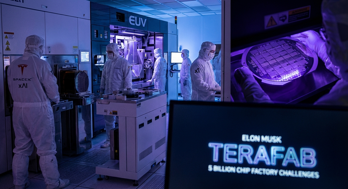
On March 21, 2026, Elon Musk unveiled Terafab — a $20–25 billion joint semiconductor fabrication venture between Tesla, SpaceX, and xAI that aims to produce more than one terawatt of AI compute capacity per year. The facility, planned for the North Campus of Giga Texas in Austin, would consolidate every stage of chip production — design, lithography, fabrication, memory production, advanced packaging, and testing — under a single roof. If realized, it would be the largest semiconductor fab ever built, by an extraordinary margin.
Musk's rationale is straightforward but staggering in scale: he claims all existing fabrication facilities on Earth produce only about 2% of what he would need across Tesla vehicles, Optimus robots, xAI's Grok models, and SpaceX's planned constellation of one million AI data center satellites. The fab would target 2-nanometer process technology — the most advanced node currently entering commercial production — with an initial capacity of 100,000 wafer starts per month, scaling to 1 million. For context, that full-scale target would represent roughly 70% of TSMC's entire current global output from a single facility.
But here's the reality that every semiconductor expert understands: building a leading-edge chip fab is arguably the most complex industrial undertaking humanity has ever attempted. It's not just about money — although the money involved is staggering. It's about mastering dozens of interrelated disciplines simultaneously, each of which takes decades to get right. Let's examine what Musk is actually up against.
Challenge 1: The Sheer Cost and Timeline. A single 2nm fab with 50,000 wafer starts per month costs roughly $28 billion, and it takes approximately 38 months just to build in the United States — from permitting and design to first wafer production. By comparison, the same fab takes about 20 months in Taiwan. TSMC spent $165 billion over years to build six fabs in Arizona, and those won't reach 2nm production until 2029. Even building in the U.S. costs 30–50% more than in Asia due to complex regulatory processes, strong construction unions, and a workforce less experienced in fab construction. Bernstein, a premier semiconductor analysis firm, estimates that Musk's full-scale ambitions could eventually require $5 trillion in total investment — more than 70% of the entire U.S. government's annual budget.
Challenge 2: Zero Semiconductor Manufacturing Experience. Tesla has never fabricated a single chip. Designing chips (which Tesla does well for Autopilot) and manufacturing them are entirely different disciplines. The closest parallel is Tesla's 4680 battery cell program: six years after Battery Day in 2020, Tesla still hasn't delivered on most of its original promises — and battery cell manufacturing is considered far simpler than leading-edge semiconductor fabrication. A semiconductor fab operates at the atomic scale, where a single particle of dust can destroy an entire wafer worth tens of thousands of dollars.
Challenge 3: The Equipment Bottleneck. A 2nm fab requires ASML Extreme Ultraviolet (EUV) lithography scanners — machines that cost over $150 million each and are made by only one company on Earth, headquartered in the Netherlands. ASML has a two-year-plus order backlog. Each scanner weighs 180 tons, requires 40 freight containers to ship, and takes months to install and calibrate. A single fab needs dozens of them. Building Terafab doesn't eliminate supply chain dependence — it shifts it to an even more concentrated set of suppliers. Beyond EUV scanners, semiconductor manufacturing relies on over 500 types of specialized equipment from companies like Applied Materials, Lam Research, KLA, and Tokyo Electron.
Challenge 4: The Workforce Crisis. A leading-edge fab requires thousands of highly specialized engineers and technicians: EUV lithographers, process integration engineers, yield engineers, equipment engineers, materials scientists, and cleanroom technicians. According to SEMI, more than 60,000 chip design and manufacturing jobs are expected to remain unfilled in the U.S. until 2030. These aren't positions you can fill with general-purpose engineers — they require years of specialized training and hands-on fab experience. TSMC, Samsung, and Intel have decades of accumulated institutional knowledge that simply cannot be replicated by hiring from job boards. Even TSMC's own Arizona expansion was delayed because, in the words of chairman Mark Liu, there was an 'insufficient amount of skilled workers.'
Challenge 5: The Cleanroom and Infrastructure Demands. A semiconductor fab cleanroom maintains air quality at Class 1 to Class 1000 standards — meaning fewer than 1,000 particles per cubic foot. For reference, a typical office has about 1 million. The cleanroom requires 600 air changes per hour, compared to 6 in a normal building. Construction alone involves 30–40 million labor hours, 83,000 tons of steel, 5,600 miles of electrical wiring, and 785,000 cubic yards of concrete. The facility consumes 30–50 megawatts of power — equivalent to a small city — and uses millions of gallons of ultra-pure water daily. Producing 1,000 gallons of the ultra-pure water required for fabrication takes 1,400–1,600 gallons of municipal water input. An individual fab's water consumption equals the daily household usage of a city of 122,000 people.
Challenge 6: Yield Engineering — The Silent Killer. Even after building the fab, installing the equipment, and hiring the workforce, the hardest part begins: achieving economically viable yields. When a new process node launches, initial yields can be as low as 20–30%, meaning 70–80% of chips on each wafer are defective. Getting to production-worthy yields of 80%+ requires years of iterative optimization by experienced process engineers. It's a discipline built on institutional knowledge — TSMC's yield engineering team has been refining their processes for over 35 years. This is what NVIDIA CEO Jensen Huang was referring to when he publicly warned Musk that matching TSMC's capabilities is 'virtually impossible.' You can buy the machines, but you can't buy the expertise to run them at peak efficiency.
Challenge 7: Chemical Supply Chain and Safety. Beneath every fab lies the sub-fab — a massive infrastructure housing ultra-pure water systems, chemical distribution networks, and gas handling facilities. Chip manufacturing uses hundreds of hazardous chemicals and gases including hydrofluoric acid, arsine, phosphine, and silane. TSMC's Arizona operation discovered that even chemical supply costs are dramatically higher in the U.S. — the company had to ship sulfuric acid from Taiwan to Los Angeles and truck it to Arizona because local suppliers couldn't meet purity requirements. Managing this chemical infrastructure safely requires an entirely separate layer of expertise and regulatory compliance.
Challenge 8: The TSMC Arizona Precedent. Perhaps the most telling indicator of Terafab's challenges is TSMC's own experience in Arizona. The world's most experienced chipmaker — with 35+ years of fab operations — has faced repeated delays, cost overruns, workforce shortages, and cultural clashes at its Phoenix site. The first fab was delayed from 2024 to late 2025. The second fab slipped from 2026 to 2027–2028. TSMC CEO C.C. Wei attributed delays to complex compliance requirements, local construction regulations, and permitting processes that take at least twice as long as in Taiwan. If TSMC struggles this much building in the U.S., the obstacles for a company with zero fab experience are exponentially greater.
What Could Go Right. None of this means Terafab is impossible. Musk has defied skeptics before — with SpaceX rocket landings, Tesla's electric vehicle revolution, and Starlink's satellite internet constellation. His planned staged approach is sensible: first building a prototype 'Advanced Technology Fabrication' facility at Giga Texas to iterate quickly before committing to the full-scale Terafab. Tesla's existing chip design expertise (the AI4 and upcoming AI5 inference chips) provides a foundation, and the vertical integration model — designing and manufacturing under one roof — could offer advantages in speed and optimization that fabless companies don't have. SpaceX's acquisition of xAI in an all-stock deal in February 2026, valuing SpaceX at $1.25 trillion, gives the combined entity the financial firepower to attempt it.
The Bottom Line. Terafab represents one of the most audacious industrial bets in history. The semiconductor industry has spent seven decades and trillions of dollars building the manufacturing capabilities that exist today. Musk is proposing to replicate and exceed them in a fraction of that time. Morgan Stanley projects that even under the most aggressive scenario, initial chip output won't occur until mid-2028 at the earliest. The challenges — cost, experience, equipment, workforce, yield, chemicals, infrastructure — are each individually daunting. Together, they define what may be the single most difficult manufacturing challenge any private company has ever undertaken. Whether Terafab succeeds or fails, it will reshape the conversation about who can — and who should — manufacture the chips that power our world.
Sources
Reuters, Bloomberg, Tom's Hardware, TechCrunch, Euronews, SEMI, Electrek, Manufacturing Dive, Semiconductor Engineering