imec Installs ASML's $400M High-NA EUV Tool, Targets Sub-2nm Qualification by Q4 2026
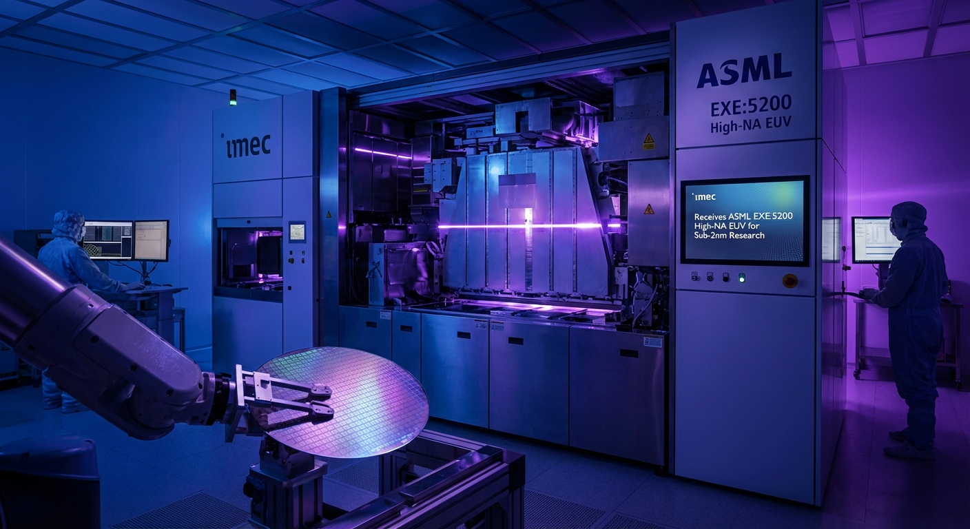
Belgian semiconductor research institute imec has taken delivery of ASML's Twinscan EXE:5200, a High-NA EUV lithography system priced at approximately $400 million and installed in imec's 300mm cleanroom in Leuven, Belgium. The tool is one of fewer than a dozen units worldwide and features a 0.55 numerical aperture (NA) optical system capable of printing features with 8nm resolution in a single exposure — compared to 13nm for conventional Low-NA EUV without multi-patterning. Overlay performance is rated at 0.7nm, a critical metric for stacking multiple patterning layers in sub-2nm logic and next-generation DRAM.
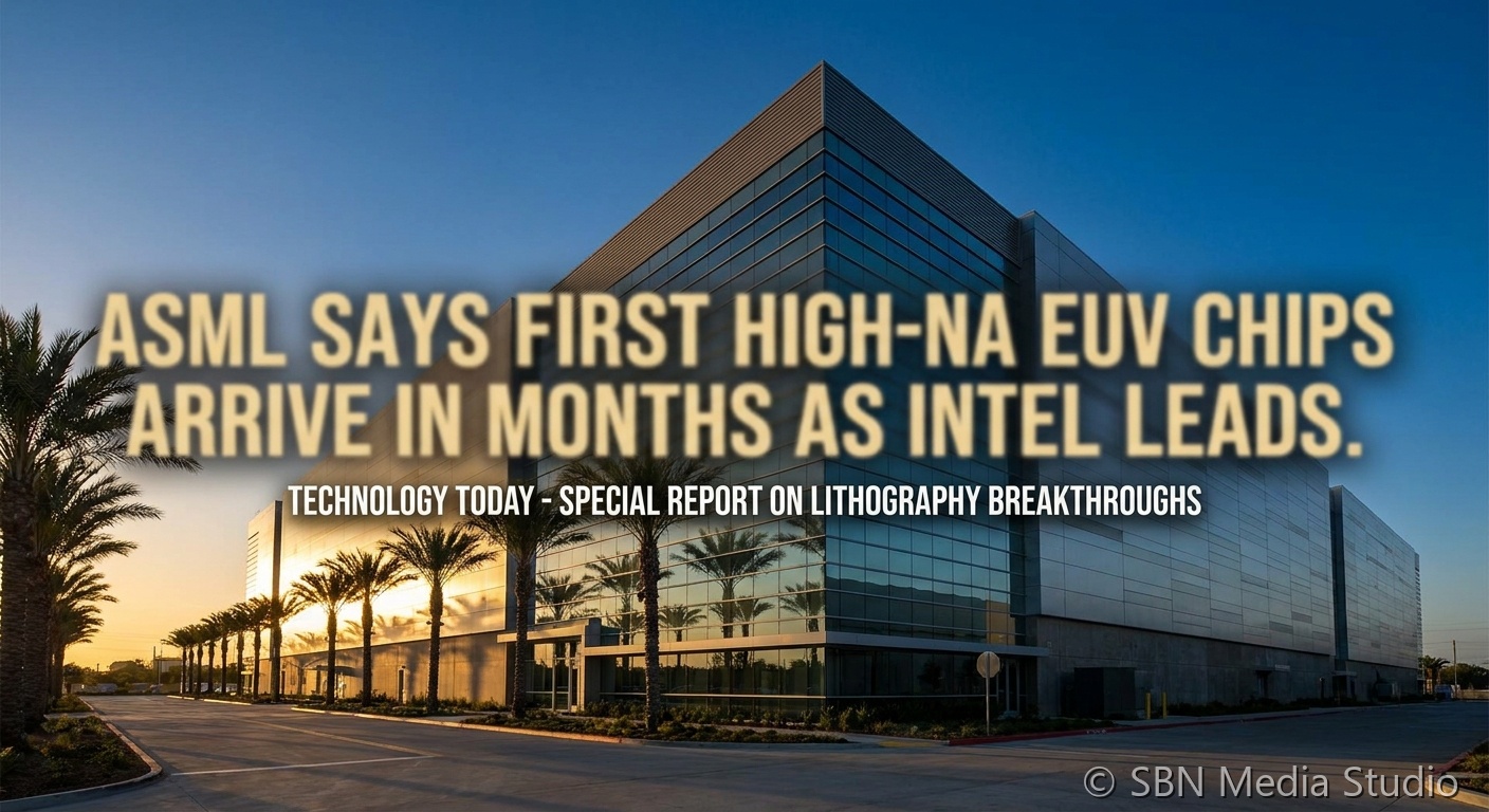
imec is targeting full tool qualification by Q4 2026, after which it will open the EXE:5200 to its global partner ecosystem — which includes TSMC, Intel, Samsung, SK Hynix, and Micron — for process development on sub-2nm logic and advanced DRAM nodes. The installation is a milestone in imec's five-year strategic partnership with ASML, co-funded by the EU Chips Joint Undertaking and the IPCEI Microelectronics program. ASML CEO Christophe Fouquet has projected industry-wide High-NA high-volume manufacturing (HVM) in 2027-2028, with Intel's 14A node among the first to commit to the tool in production.
The competitive dynamic around High-NA is nuanced. TSMC has explicitly chosen to skip High-NA EUV for its 2nm (N2) and A16 process nodes, instead extending its existing Low-NA fleet with multi-patterning — a decision that reduces capital expenditure but requires more process steps. Intel, by contrast, has installed the world's first commercial High-NA unit (the EXE:5200B) at its Oregon fab and is integrating it into the 14A node roadmap. imec's neutral, pre-competitive role means its qualification work on the EXE:5200 will benefit all partners simultaneously, potentially accelerating the industry's transition and giving TSMC optionality to adopt High-NA for its A14 and beyond process nodes after 2027.
Sources
TrendForce, Tom's Hardware