SK Hynix Breaks Ground on World's Largest HBM Packaging Plant With $13 Billion Investment
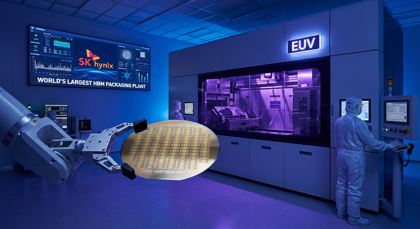
SK Hynix has commenced construction on its P&T7 (Packaging & Testing 7) facility in Cheongju, South Korea — a 19 trillion won ($12.9 billion) advanced packaging plant that will become the largest HBM assembly and test facility in the world upon completion. Spanning approximately 231,000 square meters, P&T7 dwarfs SK Hynix's existing $3.9 billion Indiana packaging site (39,948 sqm) by a factor of nearly six. Full operations are targeted by end of 2027, with equipment orders already placed as of February 2026.
The facility will specialize in 2.5D advanced packaging with through-silicon vias (TSVs), the stacking technology at the heart of HBM production. P&T7 will operate in physical and logistical integration with the adjacent M15X memory fab, creating an end-to-end HBM production campus. SK Hynix projects this is the worst HBM supply shortage on record, with demand from AI accelerator vendors — led by NVIDIA's Blackwell and Vera Rubin platforms — outpacing production capacity. The company currently supplies more than 50% of global HBM and is projecting HBM demand will grow at a 33% CAGR from 2025 to 2030.
The investment underscores the strategic importance of advanced packaging as a bottleneck in the AI semiconductor supply chain. Unlike logic wafer fabrication — where TSMC and Samsung are the gatekeepers — HBM packaging requires specialized TSV bonding infrastructure that takes years to build and qualify. SK Hynix's Cheongju campus will run HBM4 and future HBM4E production for clients including NVIDIA, AMD, and potentially Google TPU. TrendForce notes that the P&T7 ramp, combined with SK Hynix's existing capacity, positions the company to supply approximately 60% of global HBM output by 2028 — a dominance that could prove strategically critical if geopolitical tensions around Taiwan escalate.
Sources
TrendForce, Bloomberg, CNBC