Samsung Running Sample Tests with AMD on Second-Gen 2nm — Google TPU Team Visits Taylor Fab
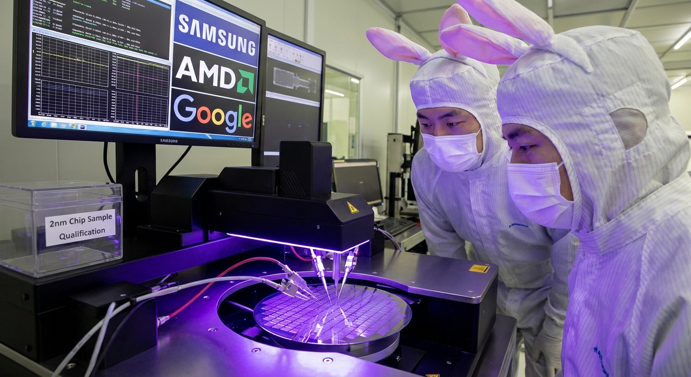
Samsung Foundry has begun running sample silicon tests with AMD on its second-generation 2nm process node, known as SF2P, which incorporates performance optimizations over the baseline SF2 technology. The SF2P process reportedly delivers an additional 5-8% performance improvement at the same power envelope, achieved through refined channel strain engineering and optimized nanosheet dimensions. The collaboration signals AMD's willingness to diversify its chip manufacturing beyond TSMC, potentially for specific product lines where capacity access matters more than cutting-edge density — a pragmatic approach given the severe allocation constraints at TSMC's most advanced nodes.
Separately, Google's TPU hardware team reportedly visited Samsung's Taylor, Texas fabrication facility to evaluate the company's readiness for producing custom AI accelerators. The Google visit is particularly notable given that TSMC's CoWoS capacity constraints have forced Google to scale back its TPU v6 production targets by an estimated 30%. Sources indicate that Google engineers spent three days at the Taylor facility, evaluating Samsung's 2nm process capabilities, advanced packaging options, and quality control systems. Samsung demonstrated its I-Cube4 packaging technology, which can integrate up to four logic dies with eight HBM stacks on a single interposer — a configuration well-suited to Google's TPU architecture.
Samsung is positioning itself as a viable second source for hyperscaler AI silicon, leveraging its integrated memory and logic capabilities as a key differentiator that neither TSMC nor Intel can match. The ability to co-optimize HBM memory and logic die manufacturing within the same company could yield performance and cost advantages for customers willing to source both from Samsung. Industry analysts estimate that if Samsung secures even one major hyperscaler AI chip contract, it could add $4-6 billion in annual foundry revenue and fundamentally alter the competitive dynamics of the advanced foundry market, where TSMC currently commands an overwhelming 90%+ share of chips below 7nm.
Sources
The Korea Herald, DigiTimes, SemiAnalysis