Samsung Unveils 2nm GAA Process — Claims 25% Power Efficiency Advantage Over TSMC N2
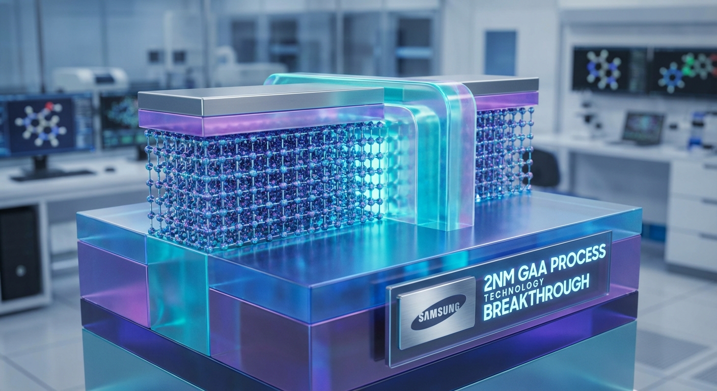
Samsung has publicly demonstrated its 2nm gate-all-around (GAA) transistor technology, claiming a 25% power efficiency advantage over TSMC's competing N2 process node. The company showcased functional test chips at its annual Samsung Foundry Forum, with mass production targeted for Q4 2026 at its Pyeongtaek campus in South Korea. The test chips demonstrated 3.2 GHz clock speeds on Arm Cortex-A730 cores, with power consumption 25% below equivalent test chips on TSMC's N2, though independent verification of these claims is still pending. Samsung's 2nm GAA process uses four-nanosheet stacks with channel widths ranging from 12nm to 45nm, enabling designers to tune performance and power on a per-transistor basis.
Qualcomm and Google have signed on as early customers, with Qualcomm expected to use the node for its next-generation Snapdragon 9 Gen 5 mobile platform and Google evaluating it for custom TPU accelerators. Samsung also announced a major expansion of its Austin, Texas fabrication facility to bring 2nm GAA production capacity to the United States, leveraging CHIPS Act incentives. The Austin expansion, valued at $12 billion, will add 30,000 wafers per month of 2nm capacity by 2028, complementing the Taylor, Texas facility's focus on automotive and AI chips. Samsung's total U.S. semiconductor investment now exceeds $56 billion, making it the second-largest foreign investor in American chip manufacturing after TSMC.
The 2nm GAA architecture replaces traditional FinFET transistors with nanosheet channels that wrap the gate around all four sides of the channel, enabling superior electrostatic control and significantly reduced leakage current at low voltages. This advantage is particularly relevant for mobile and IoT applications where battery life is paramount. If Samsung can deliver on its yield and performance claims, the 2nm GAA process could represent its strongest competitive position against TSMC in over a decade. However, skeptics point to Samsung's history of overpromising on foundry technology — its 3nm GAA node, launched in 2022, suffered persistent yield issues that drove key customer Qualcomm back to TSMC. Samsung's foundry division must demonstrate that its 2nm execution can match its 2nm ambition, and the Tesla and Qualcomm partnerships will serve as the definitive test of that proposition.
Sources
Samsung, EE Times, TrendForce, AnandTech